Maximum Collector Emitter Saturation Voltage
: 0.4 V
Minimum Operating Temperature
: - 55 C
Packaging
: Tube
Maximum Power Dissipation
: 500 mW
Maximum Operating Temperature
: + 100 C
Input Type
: DC
Maximum Forward Diode Voltage
: 1.3 V
Current Transfer Ratio
: 600 %
Isolation Voltage
: 5300 Vrms
Maximum Collector Emitter Voltage
: 70 V
Maximum Collector Current
: 100 mA
Package / Case
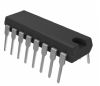
: PDIP-16
Features: • Alternate source to TLP621-2/-4 and TLP621GB-2/-4
• High collector emitter voltage, BVCEO = 70 V
• Dual and quad packages feature:
- Lower pin and parts count
- Better channel to channel CTR match
- Improved common mode rejection
• Isolation test voltage, 5300 VRMS
• Lead (Pb)-free component
• Component in accordance to RoHS 2002/95/EC and WEEE 2002/96/EC
Application• UL1577, file no. E52744 system code H or J, double protection
• DIN EN 60747-5-2 (VDE 0884)/DIN EN 60747-5-5 pending available with option 1
• BSI IEC 60950; IEC 60065
• FIMKOPinout Specifications
| PARAMETER |
TEST CONDITION |
PART |
SYMBOL |
VALUE |
UNIT |
| INPUT |
| Reverse voltage |
|
|
VR |
6.0 |
V |
| Forward current |
|
|
IF |
60 |
mA |
| Surge current |
|
|
IFSM |
1.5 |
A |
| Power dissipation |
|
|
Pdiss |
100 |
mW |
| Derate from 25 |
|
|
|
1.33 |
mW/ |
| OUTPUT |
| Collector emitter reverse voltage |
|
|
VECO |
70 |
V |
| Collector current |
|
|
IC |
50 |
mA |
| t < 1.0 ms |
|
IC |
100 |
mA |
| Power dissipation |
|
|
Pdiss |
150 |
mW |
| Derate from 25 |
|
|
|
-2.0 |
mW/ |
| COUPLER |
| Isolation test voltage |
t = 1.0 s |
|
VISO |
5300 |
VRMS |
| Package dissipation |
|
ILD621 |
|
400 |
mW |
| |
ILD621GB |
|
400 |
mW |
| Derate from 25 |
|
|
|
5.33 |
mW/ |
| Package dissipation |
|
ILQ621 |
|
500 |
mW |
| |
ILQ621GB |
|
500 |
mW |
| Derate from 25 |
|
|
|
6.67 |
mW/ |
| Creepage distance |
|
|
|
7.0 |
mm |
| Clearance distance |
|
|
|
7.0 |
mm |
| Isolation resistance |
VIO = 500 V, Tamb = 25 |
|
RIO |
1012 |
|
| VIO = 500 V, Tamb = 100 |
|
RIO |
1011 |
|
| Storage temperature |
|
|
Tstg |
- 55 to + 150 |
|
| Operating temperature |
|
|
Tamb |
- 55 to + 100 |
|
| Junction temperature |
|
|
Tj |
100 |
|
| Soldering temperature (2) |
2.0 mm from case bottom |
|
Tsld |
2600 |
|
Notes
(1) Tamb = 25 , unless otherwise specified.
Stresses in excess of the absolute maximum ratings can cause permanent damage to the device. Functional operation of the device is not implied at these or any other conditions in excess of those given in the operational sections of this document. Exposure to absolute maximum ratings for extended periods of the time can adversely affect reliability.
(2) Refer to reflow profile for soldering conditions for surface mounted devices (SMD). Refer to wave profile for soldering conditions for through hole devices (DIP).DescriptionThe ILD621/ILQ621 and ILD621GB/ILQ621GB are multi-channel phototransistor optocouplers that use GaAs IRLED emitters and high gain NPN silicon phototransistors. These devices are constructed using double molded insulation technology. This assembly process offers a withstand test voltage of 7500 VDC.
The ILD621/ILQ621GB is well suited for CMOS interfacing given the CTRCEsat of 30 % minimum at IF of 1.0 mA. High gain linear operation is guaranteed by a minimum CTRCE of 100 % at 5.0 mA. The ILD/Q621 has a guaranteed CTRCE 50 % minimum at 5.0 mA. The transparent ion shield insures stable DC gain in applications such as power supply feedback circuits, where constant DC VIO voltages are present.

 ILQ621GB Data Sheet