Maximum Collector Current
:
Minimum Operating Temperature
: - 55 C
Packaging
: Reel
Maximum Operating Temperature
: + 100 C
Maximum Power Dissipation
: 300 mW
Input Type
: DC
Maximum Collector Emitter Voltage
: 70 V
Current Transfer Ratio
: 200 %
Package / Case
: SOIC-8
Maximum Collector Emitter Saturation Voltage
: 400 mV
Maximum Forward Diode Voltage
: 1.55 V
Isolation Voltage
: 4000 Vrms
Features: • Two Channel Coupler
• SOIC-8A Surface Mountable Package
• Standard Lead Spacing of .05 "
• Available only on Tape and Reel Option (Conforms to EIA Standard 481-2)
• Isolation Test Voltage, 3000 VRMS
• Compatible with Dual Wave, Vapor Phase and IR Reflow Soldering
• Lead-free component
• Component in accordance to RoHS 2002/95/EC and WEEE 2002/96/ECApplication• UL1577, File No. E52744 System Code YPinout
 Specifications
| Parameter |
Test condition |
Symbol |
Value |
Unit |
| Peak reverse voltage |
|
VR |
6.0 |
V |
| Peak pulsed current |
1.0 µs, 300 pps |
|
1.0 |
mA |
Continuous forward current per
channel |
|
|
30 |
A |
| Power dissipation |
|
Pdiss |
50 |
mW |
| Derate linearly from 25 °C |
|
|
0.66 |
mW/°C |
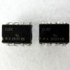
DescriptionThe ILD205T/ 206T/ 207T/ 211T/ 213T/ 217T are optically coupled pairs with a Gallium Arsenide infrared LED and a silicon NPN phototransistor. Signal information, including a DC level, can be transmitted by the device while maintaining a high degree of electrical isolation between input and output. The ILD205T/ 206T/ 207T/ 211T/ 213T/ 217T come in a standard SOIC-8A small outline package for surface mounting which makes ILD207T ideally suited for high density applications with limited space. In addition to eliminating through-holes requirements, this package conforms to standards for surface mounted devices.
A specified minimum and maximum CTR ILD207T allows a narrow tolerance in the electrical design of the adjacent circuits. The high BVCEO of 70 V gives a higher safety margin compared to the industry standard of 30 V.
The ILD207T is designed as one kind of dual channel optocoupler that can be used for high density applications with limited space. And this device has some points of features: (1)Two Channel Coupler; (2)SOIC-8A Surface Mountable Package; (3)Standard Lead Spacing of .05 "; (4)Available only on Tape and Reel Option (Conforms to EIA Standard 481-2); (5)Isolation Test Voltage, 3000 VRMS; (6)Compatible with Dual Wave, Vapor Phase and IR Reflow Soldering; (7)Lead-free component.
The absolute maximum ratings of the ILD207T can be summarized as:(1)Peak reverse voltage: 6.0 V;(2)Peak pulsed current: 1.0 A;(3)Continuous forward current per channel: 30 mA;(4)Power dissipation: 50 mW;(5)Derate linearly from 25 °C: 0.66 mW/°C;(6)Collector-emitter breakdown voltage: 70 V;(7)Emitter-collector breakdown voltage: 7.0 V;(8)Power dissipation per channel: 125 mW;(9)Derate linearly from 25 °C: 1.67 mW/°C.etc.
The electrical characteristics of ILD207T can be summarized as:(1)Forward voltage: 1.2 to 1.55 V;(2)Reverse current: 0.1 to 100 A;(3)input capacitance: 25 pF;(4)Collector-emitter breakdown voltage: 70 V;(5)Emitter-collector breakdown voltage: 7.0 V;(6)Collector-emitter leakage current: 5.0 to 50 nA;(7)Collector-emitter capacitance: 10 pF;(8)Collector-emitter saturation voltage: 0.4 V;(9)Capacitance (input-output): 0.5 pF.etc. If you want to know more information about the ILD207T, please download the datasheet in www.seekic.com or www.chinaicmart.com .

 ILD207T Data Sheet


