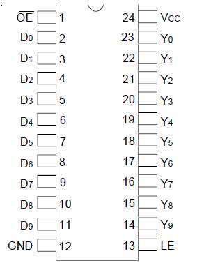
Features: • CMOS power levels: <7.5mW static• Undershoot clamp diodes on all outputs• True TTL input and output compatibility• Ground bounce controlled outputs• Reduced output swing of 0 to 3.5V• Built-in 25 series resistor outputs reduce reflection and other...
IDTQS74FCT2841AT: Features: • CMOS power levels: <7.5mW static• Undershoot clamp diodes on all outputs• True TTL input and output compatibility• Ground bounce controlled outputs• Redu...
SeekIC Buyer Protection PLUS - newly updated for 2013!
268 Transactions
All payment methods are secure and covered by SeekIC Buyer Protection PLUS.
Symbol |
Description |
Max |
Unit |
VTERM |
Terminal Voltage with Respect to GND |
0.5 to +7 |
V |
TSTG |
Storage Temperature |
65 to +150 |
°C |
IOUT |
DC Output Current Max Current Sink/Pin |
+120 |
mA |
IIK |
Input Diode Current, VIN < 0 |
-20 |
mA |
IOK |
DC Output Current, VOUT < 0 |
-50 |
mA |
NOTE:
1. Stresses greater than those listed under ABSOLUTE MAXIMUM RATINGS may cause permanent damage to the device. This is a stress rating only and functional operation of the device at these or any other conditions above those indicated in the operational sections of this specification is not implied. Exposure to absolute maximum rating conditions for extended periods may affect reliability.
The IDTQS74FCT2841AT is a 10-bit high-speed CMOS TTL-compatible buffered latch with 3-state outputs, with a 25 resister that is useful for driving transmission lines and reducing system noise. The 2841 eliminates the need for external series resistors in high speed systems and can replace the 841 series to reduce noise in an existing design. All inputs have clamp diodes for undershoot noise suppression. All outputs have ground bounce suppression. Outputs will not load an active bus when Vcc is removed from the device.