Features: · Full featured single chip M13-ideal for upgrading existing multi-line T1/E1 line cards to single line channelized T3 service· Small footprint 17mm x 17mm BGA package and 208 pin PQFP packages available· 3.3V operation with 5V tolerant I/O· 28 independent DS1 clock inputs each with prog...
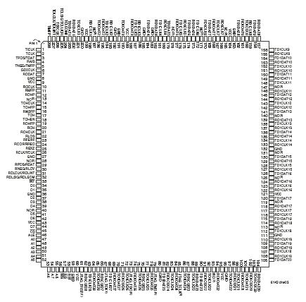
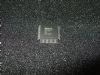
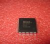
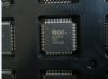
IDT82V8313: Features: · Full featured single chip M13-ideal for upgrading existing multi-line T1/E1 line cards to single line channelized T3 service· Small footprint 17mm x 17mm BGA package and 208 pin PQFP pac...
SeekIC Buyer Protection PLUS - newly updated for 2013!
268 Transactions
All payment methods are secure and covered by SeekIC Buyer Protection PLUS.
1.4.1 Reframing
1.4.1.1 Procedure
The search of frame alignment must be activated in three cases:
· After a reset.
· When the microprocessor forced the reframing process.
· After an internal out of frame (OOF) declaration (but reframing
asked by microprocessor). When a DS2 reframing is in process, Allones AIS signal is sent downstream for the duration of the reframing.
1.4.1.2 Max Time
For G.747 applications the DS2 framer has a maximum reframe rime of less than 1ms. In order for the framer to declare framing however, the candidate frame alignment signal must be present for 3 consecutive frames in accordance with CCITT Rec. G.747 Section 4. Once in frame the DS2 framer will provide frame boundary indications as well as overhead bit positions.
1.4.2 Alarms and errors
1.4.2.1 OOF
For alarm indications the DS2 framer is designed to indicate OOF conditions when 4 consecutive frame alignment signals are incorrect in accordance with CCITT Rec. G.747 Section 4. Much like the DS3 framer, the DS2 framer is an "off-line" framer and will continue to indicate errors when OOF based on the previous frame alignment.
1.4.2.2 AIS
In G.747 applications the DS2 framer also uses an integration algorithm with a 1:1 slope to detect RED alarm and AIS. Instead of using DS2 frames however the DS2 framer uses G.747 frames with the integrator counter. AIS is defined as the occurrence of less than 9 zeros while the framer is OOF during that G.747-frame. RED alarm is defined as the detection of a RED defect, or OOF in an M-frame. For each interval, a G.747 frame, if the framer detects a Red defect or AIS event, the integrator counter is incremented. Accordingly, if a valid G.747 frame is received then integrator counter is decremented. As a result the DS2 Framer can detect RED alarm and AIS in 6.9ms.
1.4.2.3 RAI
The DS2 framer also extracts the DS2 X-bit and G.747 Remote Alarm Indication bit, RAI, to indicate a Far End Receive Failure, FERF.
The DS2 framer uses an internal status FIFO to insure that for an OOF condition, nearly 100% of the time for DS2 applications and 99.9% of the time for G.747 applications, that the DS2 framer will freeze in a valid state. If two successive X-bits or RAI bits are the same, then a FERF status is indicated and entered into the internal status FIFO. Each M-frame or G.747 frame the status FIFO will be updated and shifted. After a total of six M-frames or G.747 frames, the error condition will reach the sixth (last) position of the FIFO. When the error condition reaches the last position in the FIFO, the DS2 Status Register will be updated to indicate to the controller that a FERF has occurred. The error indication/value will be held in that sixth(last) position while the fifth through second positions will freeze the FERF state of the four M-frames following the FERF condition. The first position of the status FIFO will contain the present FERF state and will be continually updated with the present FERF status. Once correct frame alignment has been reestablished and the OOF condition is gone, then the first FIFO status location will have a valid indication. At this point the FIFO will continue to operate normally, by shifting the FERF status through the FIFO.
Symbol | Parameter | Min. | Max. | Unit |
Vcc | Supply Voltage | -0.5 | +43.0 | V |
VI | Voltage on Digital Inputs | GND -0.3 | Vcc +0.3 | V |
Io | Current at Digital Outputs | -50 | 50 | mA |
Ts | Storage Temperature | -55 | +125 | °C |
PD | Package Power Dissipation | - | 2 | W |
Ambient Temperature under Bias | -40 | +85 | °C | |
Static Discharge Voltage | -500 | +500 | V | |
Latch-Up Current | -100 | +100 | mA | |
Lead Temperature | - | +300 | °C | |
Absolute Maximum Junction Temperature | - | +150 | °C |