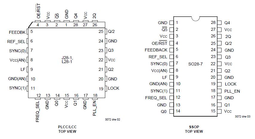
Features: • 0.5 MICRON CMOS Technology
• Input frequency range: 10MHz f2Q Max. spec (FREQ_SEL = HIGH)
• Max. output frequency: 133MHz
• Pin and function compatible with MC88915T
• 5 non-inverting outputs, one inverting output, one 2x output, one ¸2 output; all outputs are TTL-compatible
• 3-State outputs
• Output skew < 500ps (max.)
• Duty cycle distortion < 500ps (max.)
• Part-to-part skew: 1ns (from tPD max. spec)
• TTL level output voltage swing
• 64/15mA drive at TTL output voltage levels
• Available in 28 pin PLCC, LCC and SSOP packagesPinout Specifications
|
Symbol |
Rating |
Commercial |
Military |
Unit |
|
VTERM(2) |
Terminal Voltage
with Respect to
GND |
0.5 to +7.0 |
0.5 to +7.0 |
V |
|
VTERM(3) |
Terminal Voltage
with Respect to
GND |
0.5 to VCC
+0.5 |
0.5 to VCC
+0.5 |
V |
|
TA |
Operating
Temperature |
0 to +70 |
55 to +125 |
°C |
|
TBIAS |
Temperature
Under Bias |
55 to +125 |
65 to +135 |
°C |
|
TSTG |
Storage
Temperature |
55 to +125 |
65 to +150 |
°C |
|
IOUT |
DC Output
Current |
60 to +120 |
60 to +120 |
mA |
DescriptionThe IDT74FCT88915TT uses phase-lock loop technology to lock the frequency and phase of outputs to the input reference clock. It provides low skew clock distribution for high performance PCs and workstations. One of the outputsis fed back to the PLL at the FEEDBACK input resulting in essentially delay across the device. The PLL consists of the phase/frequency detector, charge pump, loop filter and VCO. The VCO is designed for a 2Q operating frequency range of 40MHz to f2Q Max.
The IDT74FCT88915TT provides 8 outputs with 500ps skew. The
Q5 output is inverted from the Q outputs. The 2Q
runs at twice the Q frequency and Q/2 runs at half the Q frequency.
The FREQ_SEL control provides an additional ¸ 2 option in the output path. PLL _EN allows bypassing of the PLL, which is useful in static test modes. When PLL_EN is low, SYNC input may be used as a test clock. In this test mode, the input frequency is not limited to the specified range and the polarity of outputs is complementary to that in normal operation (PLL_EN = 1). The LOCK output attains logic HIGH when the PLL is in steady-state phase and frequency lock. When OE/
RST is low, all the outputs are put in high impedance state and registers at Q,
Q and Q/2 outputs are reset.
The IDT74FCT88915TT requires one external loop filter component as recommended in Figure 1.

 IDT74FCT88915TT Data Sheet


