IDT74FCT388915T

Features: • 0.5 MICRON CMOS Technology• Input frequency range: 10MHz f2Q Max. spec (FREQ_SEL = HIGH)• Max. output frequency: 150MHz• Pin and function compatible with FCT88915T, MC88915T• 5 non-inverting outputs, one inverting output, one 2x output, one÷2 output; all ...

product image

IDT74FCT388915T Picture
SeekIC No. : 004373046 Detail

IDT74FCT388915T: Features: • 0.5 MICRON CMOS Technology• Input frequency range: 10MHz f2Q Max. spec (FREQ_SEL = HIGH)• Max. output frequency: 150MHz• Pin and function compatible with FCT8891...

floor Price/Ceiling Price

Part Number:
IDT74FCT388915T
Supply Ability:
5000

Price Break

  • Qty
  • 1~5000
  • Unit Price
  • Negotiable
  • Processing time
  • 15 Days
Total Cost: $ 0.00

SeekIC Buyer Protection PLUS - newly updated for 2013!

  • Escrow Protection.
  • Guaranteed refunds.
  • Secure payments.
  • Learn more >>

Month Sales

268 Transactions

Rating

evaluate  (4.8 stars)

Upload time: 2024/11/24

Payment Methods

All payment methods are secure and covered by SeekIC Buyer Protection PLUS.

Notice: When you place an order, your payment is made to SeekIC and not to your seller. SeekIC only pays the seller after confirming you have received your order. We will also never share your payment details with your seller.
Product Details

Description


Features:

• 0.5 MICRON CMOS Technology
• Input frequency range: 10MHz f2Q Max. spec (FREQ_SEL = HIGH)
• Max. output frequency: 150MHz
• Pin and function compatible with FCT88915T, MC88915T
• 5 non-inverting outputs, one inverting output, one 2x output, one÷2 output; all outputs are TTL-compatible
• 3-State outputs
• Output skew < 350ps (max.)
• Duty cycle distortion < 500ps (max.)
• Part-to-part skew: 1ns (from tPD max. spec)
• 32/16mA drive at CMOS output voltage levels
• VCC = 3.3V ± 0.3V
• Inputs can be driven by 3.3V or 5V components
• Available in 28 pin PLCC, LCC and SSOP packages


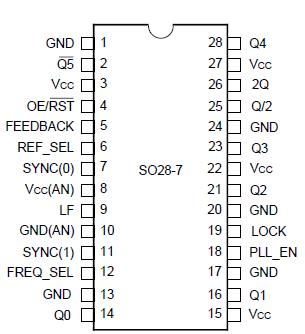
Pinout

  Connection Diagram


Specifications

Symbol Description
Commercial

Military
Unit
VTERM(2) Terminal Voltage with Respect to GND
0.5 to +4.6
-0.5 to +4.6
V
VTERM(3) Terminal Voltage with Respect to GND
0.5 to +7.0
0.5 to +7.0
V
VTERM(4) Terminal Voltage with Respect to GND
0.5 to VCC
+0.5
0.5 to VCC
+0.5
V
TA Operating Temperature
0 to +70
55 to +125
TBIAS Temperature Under Bias
55 to +125
65 to +135
TSTG Storage Temperature
55 to +125
65 to +150
IOUT DC Output Current
60 to +60
60 to +60
mA

NOTES: 1. Stresses greater than those listed under ABSOLUTE MAXIMUM RATINGS may cause permanent damage to the device. This is a stress rating only and functional operation of the device at these or any other conditions above those indicated in the operational sections of this specification is not implied. Exposure to absolute maximum rating conditions for extended periods may affect reliability.
2. Vcc terminals.
3. Input terminals.
4. Output and I/O terminals.


Description

The IDT54/74FCT388915T uses phase-lock loop technology to lock the frequency and phase of outputs to the input reference clock. IDT74FCT388915T provides low skew clock distribution for high performance PCs and workstations. One of the outputs is fed back to the PLL at the FEEDBACK input resulting in essentially zero delay across IDT74FCT388915T. The PLL consists of  the phase/frequency detector, charge pump, loop filter and VCO. The VCO of IDT74FCT388915T is designed for a 2Q operating frequency range of 40MHz to f2Q Max.

The IDT54/74FCT388915T provides 8 outputs with 350ps  skew. The Q5 output is inverted from the Q outputs. The 2Q runs at twice the Q frequency and Q/2 runs at half the Q frequency.

The FREQ_SEL control provides an additional ¸ 2 option in the output path. PLL _EN allows bypassing of the PLL, which is useful in static test modes. When PLL_EN is low, SYNC input may be used as a test clock. In this test mode, the input frequency is not limited to the specified range and the polarity of outputs is complementary to that in normal operation (PLL_EN = 1). The LOCK output attains logic HIGH when the PLL is in steady-state phase and frequency lock. When OE/ RST is low, all the outputs are put in high impedance state and registers at Q, Q and Q/2 outputs are reset.

The IDT54/74FCT388915T requires one external loop filter component as recommended in Figure 3.


Customers Who Bought This Item Also Bought

Margin,quality,low-cost products with low minimum orders. Secure your online payments with SeekIC Buyer Protection.
Crystals and Oscillators
Motors, Solenoids, Driver Boards/Modules
Industrial Controls, Meters
Cables, Wires
Power Supplies - External/Internal (Off-Board)
Isolators
View more