IDT74FCT16543CT

Features: • 0.5 MICRON CMOS Technology• High-speed, low-power CMOS replacement for ABT functions• Typical tSK(o) (Output Skew) < 250ps• Low input and output leakage 1A (max.)• VCC = 5V ±10%• High drive outputs (32mA IOH, 64mA IOL)• Power off disable out...

product image

IDT74FCT16543CT Picture
SeekIC No. : 004372956 Detail

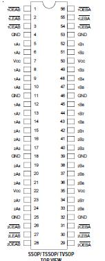
IDT74FCT16543CT: Features: • 0.5 MICRON CMOS Technology• High-speed, low-power CMOS replacement for ABT functions• Typical tSK(o) (Output Skew) < 250ps• Low input and output leakage 1A (ma...

floor Price/Ceiling Price

Part Number:
IDT74FCT16543CT
Supply Ability:
5000

Price Break

  • Qty
  • 1~5000
  • Unit Price
  • Negotiable
  • Processing time
  • 15 Days
Total Cost: $ 0.00

SeekIC Buyer Protection PLUS - newly updated for 2013!

  • Escrow Protection.
  • Guaranteed refunds.
  • Secure payments.
  • Learn more >>

Month Sales

268 Transactions

Rating

evaluate  (4.8 stars)

Upload time: 2024/6/4

Payment Methods

All payment methods are secure and covered by SeekIC Buyer Protection PLUS.

Notice: When you place an order, your payment is made to SeekIC and not to your seller. SeekIC only pays the seller after confirming you have received your order. We will also never share your payment details with your seller.
Product Details

Description


Features:

• 0.5 MICRON CMOS Technology
• High-speed, low-power CMOS replacement for ABT functions
• Typical tSK(o) (Output Skew) < 250ps
• Low input and output leakage 1A (max.)
• VCC = 5V ±10%
• High drive outputs (32mA IOH, 64mA IOL)
• Power off disable outputs permit "live insertion"
• Typical VOLP (Output Ground Bounce) < 1.0V at VCC = 5V, TA = 25°C
• Available in SSOP, TSSOP, and TVSOP packages


Pinout

  Connection Diagram


Specifications

Symbol

Description
Max
Unit
VTERM(2)
Terminal Voltage with Respect to GND
0.5 to +7
V
VTERM(3)
Terminal Voltage with Respect to GND
0.5 to VCC+0.5
V
TSTG
Storage Temperature
65 to +150
°C

IOUT

DC Output Current
60 to +120
mA

NOTES:
1. Stresses greater than those listed under ABSOLUTE MAXIMUM RATINGS may cause permanent damage to the device. This is a stress rating only and functional operation of the device at these or any other conditions above those indicated in the operational sections of this specification is not implied. Exposure to absolute maximum rating conditions for extended periods may affect reliability.
2. All device terminals except FCT162XXX Output and I/O terminals.
3. Output and I/O terminals for FCT162XXX.


Description

The IDT74FCT16543CT 16-bit latched transceivers are built using advanced dual metal CMOS technology. These high-speed, low-power devices are organized as two independent 8-bit D-type latched transceivers with separate input and output control to permit independent control of data flow in either direction. For example, the A-to-B Enable (xCEAB) must be low in order to enter data from the A port or to output data from the B port. xLEAB controls the latch function. When xLEAB is low, the latches are transparent. A subsequent low-to-high transition of xLEAB signal puts the A latches in the storage mode. xOEAB performs output of the IDT74FCT16543CT enable function on the B port. Data flow from the B port to the A port is similar but requires using xCEBA, xLEBA, and xOEBA inputs. Flow-through organization of signal pins simplifies layout. All inputs are designed with hysteresis for improved noise margin.

The IDT74FCT16543CT is ideally suited for driving high-capacitance loads and low-impedance backplanes. The output buffers are designed with power off disable capability to allow "live insertion" of boards when used as backplane drivers.


Customers Who Bought This Item Also Bought

Margin,quality,low-cost products with low minimum orders. Secure your online payments with SeekIC Buyer Protection.
RF and RFID
Memory Cards, Modules
Batteries, Chargers, Holders
Crystals and Oscillators
Cables, Wires
View more