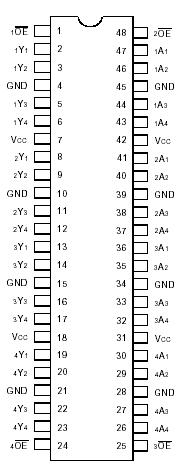
Features: • 0.5 MICRON CMOS Technology• Typical tSK(o) (Output Skew) < 250ps• ESD > 2000V per MIL-STD-883, Method 3015; > 200V using machine model (C = 200pF, R = 0)• VCC = 3.3V ± 0.3V, Normal Range• VCC = 2.7V to 3.6V, Extended Range• VCC = 2.5V ± 0.2V...
IDT74ALVCH162821: Features: • 0.5 MICRON CMOS Technology• Typical tSK(o) (Output Skew) < 250ps• ESD > 2000V per MIL-STD-883, Method 3015; > 200V using machine model (C = 200pF, R = 0)•...
SeekIC Buyer Protection PLUS - newly updated for 2013!
268 Transactions
All payment methods are secure and covered by SeekIC Buyer Protection PLUS.
Symbol |
Rating |
Max
|
Unit |
VTERM (VDD) |
VDD Terminal Voltage with Respect to GND |
0.5 to +4.6 |
V |
VTERM(2) |
VDDQ Terminal Voltage with Respect to GND |
0.5 to VCC+0.5 |
V |
VTERM(2) (INPUTS and I/O's) |
Input and I/O Terminal Voltage with Respect to GND |
65 to +150
|
°C |
IOUT |
DC Output Current |
50 to +50
|
°C |
TSTG |
Continuous Clamp Current, VI < 0 or VI > VCC |
-65 to +150
|
mA |
TJN |
Junction Temperature |
+ 150
|
mA |
IOK |
Continuous Clamp Current, VO < 0 |
-50
|
mA |
ICC ISS |
Continuous Current through VCC or GND |
±100
|
mA |
NOTES:
1. Stresses greater than those listed under ABSOLUTE MAXIMUM RATINGS may cause permanent damage to the device. This is a stress rating only and functional operation of the device at these or any other conditions above those indicated in the operational sections of this specification is not implied. Exposure to absolute maximum rating conditions for extended periods may affect reliability.
2. VCC terminals.
3. All terminals except VCC.
This 20-bit bus-interface flip-flop of the IDT74ALVCH162821 is built using advanced CMOS technology. The ALVCH162821 device can be used as two 10-bit flip-flops or one 20-bit flip-flop.
The 20-bit flip-flops of the IDT74ALVCH162821 are edge-triggered D-type flip-flops. On the positive transition of the clock (CLK) input, the device provides true data at the Q outputs. A buffered output-enable (OE) input can be used to place the ten outputs in either a normal logic state (high or low logic levels) or a high-impedance state. In the high impedance state, the outputs neither load nor drive the bus lines significantly. The high-impedance state and increased drive provide the capability to drive bus lines without the need for interface or pullup components. OE input does not affect the internal operation of the flip-flops. Old data can be retained or new data can be entered while the outputs are in the high-impedance state.
The IDT74ALVCH162821 has series resistors in the device output structure which will significantly reduce line noise when used with light loads. This driver has been designed to drive ±12mA at the designated threshold levels.
The IDT74ALVCH162821 has "bus-hold" which retains the inputs' last state whenever the input goes to a high impedance. This prevents floating inputs and eliminates the need for pull-up/down resistor.