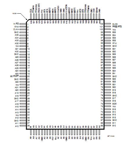
Features: Memory storage capacity:
IDT72V3684¨ C16,384 x 36 x
IDT72V3694¨ C32,768 x 36 x
IDT72V36104¨C65,536 x36 x 2
Clock frequencies up to 100 MHz (6.5ns access time)
Two independent clocked FIFOs buffering data in opposite directions
Select IDT Standard timing (using EFA, EFB, EFA, and EFB flags unctions) or First Word Fall Through Timing (using ORA, ORB,RA, and IRB flag functions)
Programmable Almost-Empty and Almost-Full flags; each has five default offsets (8, 16, 64, 256 and 1,024 )
Serial or parallel programming of partial flags
Retransmit Capability
Port B bus sizing of 36 bits (long word), 18 bits (word) and 9 bits (byte)
Big- or Little-Endian format for word and byte bus sizes
Master Reset clears data and configures FIFO, Partial Reset clears data but retains configuration settings
Mailbox bypass registers for each FIFO
Free-running CLKA and CLKB may be asynchronous or coincident (simultaneous reading and writing of data on a single clock edge is permitted)
Auto power down minimizes power dissipation
Available in space saving 128-pin Thin Quad Flatpack (TQFP)
Pin compatible to the lower density parts, IDT72V3624/72V3634/72V3644/72V3654/72V3664/72V3674
Industrial temperature range (-40°C to +85°C) is available
Pinout Specifications
| Symbol |
Rating |
Commercial |
Unit |
| VCC |
Supply Voltage Range |
-0.5 to +4.6 |
V |
| VI(2) |
I Input Voltage Range |
-0.5 to VCC+0.5 |
V |
| VO(2) |
Output Voltage Range |
-0.5 to VCC+0.5 |
V |
| IIK |
Input Clamp Current (VI < 0 or VI > VCC) |
±20 |
mA |
| IOK |
Output Clamp Current (VO = < 0 or VO > VCC) |
±50 |
mA |
| IOUT |
Continuous Output Current (VO = 0 to VCC) |
±50 |
mA |
| ICC |
Continuous Current Through VCC or GND |
±400 |
mA |
| TSTG |
Storage Temperature Range |
-65 to 150 |
|
DescriptionThe IDT72V3694 are designed to run off a 3.3V supply for exceptionally low-power consumption. These devices are mono-lithic, high-speed, low-power, CMOS bidirectional synchronous (clocked) FIFO memory which supports clock frequencies up to 100 MHz and has read access times as fast as 6.5ns. Two independent 16,384/32,768/65,536 x 36 dual-port SRAM FIFOs on board each chip buffer data in opposite directions.FIFO data on Port B can be input and output in 36-bit, 18-bit, or 9-bit formats with a choice of Big- or Little-Endian configurations.
These devices of the IDT72V3694 are a synchronous (clocked) FIFO, meaning each port employs a synchronous interface. All data transfers through a port are gated to the LOW-to-HIGH transition of a port clock by enable signals. The clocks for
each port are independent of one another and can be asynchronous or coincident. The enables for each port are arranged to provide a simple bidirectional interface between microprocessors and/or buses with synchro- nous control.
Communication of the IDT72V3694 between each port may bypass the FIFOs via two mailbox registers. The mailbox registers' width matches the selected Port B bus width

 IDT72V3694 Data Sheet


