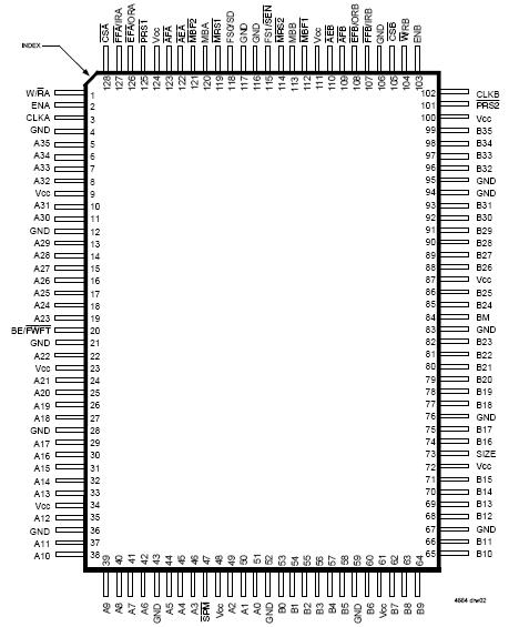
Features: • Memory storage capacity: IDT72V3624256 x 36 x 2 IDT72V3634512 x 36 x 2 IDT72V36441,024 x 36 x 2• Clock frequencies up to 100 MHz (6.5ns access time)• Two independent clocked FIFOs buffering data in opposite directions• Select IDT Standard timing (using EFA, EFB,...
IDT72V3644: Features: • Memory storage capacity: IDT72V3624256 x 36 x 2 IDT72V3634512 x 36 x 2 IDT72V36441,024 x 36 x 2• Clock frequencies up to 100 MHz (6.5ns access time)• Two independent cl...
SeekIC Buyer Protection PLUS - newly updated for 2013!
268 Transactions
All payment methods are secure and covered by SeekIC Buyer Protection PLUS.
Symbol | Rating | Commercial | Unit |
VCC | Supply Voltage Range | 0.5 to +4.6 | V |
VI(2) | Input Voltage Range | 0.5 to VCC+0.5 | V |
VO(2) | Output Voltage Range | 0.5 to VCC+0.5 | V |
IIK | Input Clamp Current (VI < 0 or VI > VCC) | ±20 | mA |
IOK | Output Clamp Current (VO = < 0 or VO > VCC) | ±50 | mA |
IOUT | Continuous Output Current (VO = 0 to VCC) | ±50 | mA |
ICC | Continuous Current Through VCC or GND | ±400 | mA |
TSTG | Storage Temperature Range | 65 to 150 | °C |
NOTES:
1. Stresses beyond those listed under "Absolute Maximum Ratings" may cause permanent damage to the device. These are stress ratings only and functional operation of the device at these or any other conditions beyond those indicated under "recommended operating conditions" is not implied. Exposure to absolute-maximum-rated conditions for extended periods may affect device reliability.
2. The input and output voltage ratings may be exceeded provided the input and output current ratings are observed.
The IDT72V3644 are pin and functionally compatible versions of the IDT723624/723634/723644, designed to run off a 3.3V supply for exceptionally low-power consumption. These devices are monolithic, highspeed, low-power, CMOS bidirectional synchronous (clocked) FIFO memory which supports clock frequencies up to 100 MHz and has read access times as fast as 6.5ns. Two independent 256/512/1,024 x 36 dual-port SRAM FIFOs on board each chip buffer data in opposite directions. FIFO data on Port B can be input and output in 36-bit, 18-bit, or 9-bit formats with a choice of Big- or Little- Endian configurations.
These devices of the IDT72V3644 are a synchronous (clocked) FIFO, meaning each port employs a synchronous interface. All data transfers through a port are gated to the LOW-to-HIGH transition of a port clock by enable signals. The clocks for each port are independent of one another and can be asynchronous or