Features: • Memory storage capacity:
IDT72V3622 256 x 36 x 2
IDT72V3632 512 x 36 x 2
IDT72V3642 1,024 x 36 x 2
• Supports clock frequencies up to 100 MHz
• Fast access times of 6.5ns
• Free-running CLKA and CLKB may be asynchronous or coincident (simultaneous reading and writing of data on a single clock edge is permitted)
• Two independent clocked FIFOs buffering data in opposite directions
• Mailbox bypass register for each FIFO
• Programmable Almost-Full and Almost-Empty flags
• Microprocessor Interface Control Logic
• FFA/IRA, EFA/ORA, AEA, and AFA flags synchronized by CLKA
• FFB/IRB, EFB/ORB, AEB, and AFB flags synchronized by CLKB
• Select IDT Standard timing (using EFA, EFB, FFA and FFB flags functions) or First Word Fall Through timing (using ORA, ORB, IRA and IRB flag functions)
• Available in 132-pin Plastic Quad Flatpack (PQFP) or space-saving 120-pin Thin Quad Flatpack (TQFP)
• Functionally compatible to the 5V operating IDT723622/723632/723642
• Industrial temperature range (40C to +85C) is availablePinout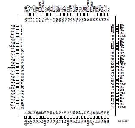 Specifications
| Symbol |
Rating |
Commercial |
Unit |
| VCC |
Supply Voltage Range |
0.5 to +4.6 |
V |
| VI(2) |
Input Voltage Range |
0.5 to VCC+0.5 |
V |
| VO(2) |
Output Voltage Range |
0.5 to VCC+0.5 |
V |
| IIK |
Input Clamp Current (VI < 0 or VI > VCC) |
±20 |
mA |
| IOK |
Output Clamp Current (VO = < 0 or VO > VCC) |
±50 |
mA |
| IOUT |
Continuous Output Current (VO = 0 to VCC) |
±50 |
mA |
| ICC |
Continuous Current Through VCC or GND |
±400 |
V |
| TSTG |
Storage Temperature Range |
65 to 150 |
|
NOTES:
1. Stresses beyond those listed under "Absolute Maximum Ratings" may cause permanent damage to the device. These are stress ratings only and functional operation of the device at these or any other conditions beyond those indicated under "recommended operating conditions" is not implied. Exposure to absolute maximum rated conditions for extended periods may affect device reliability.
2. The input and output voltage ratings may be exceeded provided the input and output current ratings are observed.DescriptionThe IDT72V3622/72V3632/72V3642 are functionally compatible versions of the IDT723622/723632/723642, designed to run off a 3.3V supply for exceptionally low-power consumption. These devices are monolithic, highspeed, low-power, CMOS Bidirectional SyncFIFO (clocked) memories which support clock frequencies up to 100MHz and have read access times as fast as 6.5ns. Two independent 256/512/1,024 x 36 dual-port SRAM FIFOs on board each chip buffer data in opposite directions. Communication between each port may bypass the FIFOs via two 36-bit mailbox registers. Each mailbox register has a flag to signal when new mail has been stored.
These devices of the IDT72V3622 are a synchronous (clocked) FIFO, meaning each port employs a synchronous interface. All data transfers through a port are gated to the LOW-to-HIGH transition of a port clock by enable signals. The clocks for each port are independent of one another and can be asynchronous or coincident. The enables for each port are arranged to provide a simple bidirectional interface between microprocessors and/or buses with synchronous control.
These devices have two modes of operation: In the IDT Standard mode, the first word written to an empty FIFO is deposited into the memory array. A read operation is required to access that word (along with all other words residing in memory). In the First Word Fall Through mode (FWFT), the first long-word (36-bit wide) written to an empty FIFO appears automatically on the outputs, no read operation required (Nevertheless, accessing subsequent words does necessitate a formal read request). The state of the FWFT pin during FIFO operation determines the mode in use.
Each FIFO of the IDT72V3622 has a combined Empty/Output Ready Flag (EFA/ORA and EFB/ORB) and a combined Full/Input Ready Flag (FFA/IRA and FFB/IRB). The EF and FF functions are selected in the IDT Standard mode. EF indicates whether or not the FIFO memory is empty. FF shows whether the memory is full or not. The IR and OR functions are selected in the First Word Fall Through mode. IR indicates whether or not the FIFO has available memory locations. OR shows whether the FIFO has data available for reading or not. It marks the presence of valid data on the outputs.
Each FIFO has a programmable Almost-Empty flag (AEA and AEB) and a programmable Almost-Full flag (AFA and AFB). AEA and AEB indicate when a selected number of words remain in the FIFO memory. AFA and AFBindicate when the FIFO contains more than a selected number of words.
FFA/IRA, FFB/IRB, AFA and AFB of the IDT72V3622 are two-stage synchronized to the port clock that writes data into its array. EFA/ORA,EFB/ORB, AEA and AEB are two-stage synchronized to the port clock that reads data from its array. Programmable offsets for AEA, AEB, AFA andAFB are loaded by using Port A. Three default offset settings are also provided. The AEA and AEB threshold can be set at 8, 16 or 64 locations from the empty boundary and the AFA and AFB threshold can be set at 8, 16 or 64 locations from the full boundary. All these choices are made using the FS0 and FS1 inputs during Reset.
Two or more devices of the IDT72V3622 may be used in parallel to create wider data paths. If, at any time, the FIFO is not actively performing a function, the chip will automatically power down. During the power down state, supply current consumption (ICC) is at a minimum. Initiating any operation (by activating control inputs) will immediately take the device out of the power down state.
The IDT72V3622/72V3632/72V3642 are characterized for operation from 0oC to 70oC. Industrial temperature range (-40C to +85C) is available by special order. They are fabricated using IDT's high speed, submicron CMOS technology.

 IDT72V3622 Data Sheet