Features: • Choose among the following memory organizations:
IDT72V281 65,536 x 9
IDT72V291 131,072 x 9
• Pin-compatible with the IDT72V261/72V271 SuperSync FIFOs
• 10ns read/write cycle time (6.5ns access time)
• Fixed, low first word data latency time
• Auto power down minimizes standby power consumption
• Master Reset clears entire FIFO
• Partial Reset clears data, but retains programmable settings
• Retransmit operation with fixed, low first word data latency time
• Empty, Full and Half-Full flags signal FIFO status
• Programmable Almost-Empty and Almost-Full flags, each flag can default to one of two preselected offsets
• Program partial flags by either serial or parallel means
• Select IDT Standard timing (using EF and FF flags) or First Word
Fall Through timing (using OR and IR flags)
• Output enable puts data outputs into high impedance state
• Easily expandable in depth and width
• Independent Read and Write clocks (permit reading and writing simultaneously)
• Available in the 64-pin Thin Quad Flat Pack (TQFP) and the 64-pin Slim Thin Quad Flat Pack (STQFP)
• High-performance submicron CMOS technology
• Industrial Temperature Range (-40°C to + 85°C) is availablePinout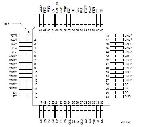 Specifications
| Symbol |
Rating |
Commercial
|
Unit |
| VTERM |
Terminal Voltage with Respect to GND |
0.5 to +4.6 |
V |
| TSTG |
Storage Temperature |
55 to +125 |
|
| IOUT |
DC Output Current |
50 to +50 |
mA |
NOTES:
1. Stresses greater than those listed under ABSOLUTE MAXIMUM RATINGS may cause permanent damage to the device. This is a stress rating only and functional operation of the device at these or any other conditions above those indicated in the operational sections of this specification is not implied. Exposure to absolute maximum rating conditions for extended periods may affect reliability.
DescriptionThe IDT72V281/72V291 are exceptionally deep, high speed, CMOS First-In-First-Out (FIFO) memories with clocked read and write controls. These FIFOs offer numerous improvements over previous SuperSync FIFOs, including the following:
• The limitation of the frequency of one clock input with respect to the other has been removed. The Frequency Select pin (FS) has been removed, thus it is no longer necessary to select which of the two clock inputs, RCLK or WCLK, is running at the higher frequency.
• The period required by the retransmit operation is now fixed and short.
• The first word data latency period, from the time the first word is written to an empty FIFO to the time it can be read, is now fixed and short. (The variable clock cycle counting delay associated with the latency period found on
previous SuperSync devices has been eliminated on this SuperSync family.)
SuperSync FIFOs of the IDT72V281 are particularly appropriate for network, video, telecommunications, data communications and other applications that need to buffer large amounts of data.
The input port of the IDT72V281 is controlled by a Write Clock (WCLK) input and a Write Enable (WEN) input. Data is written into the FIFO on every rising edge of WCLK when WEN is asserted. The output port is controlled by a Read Clock (RCLK) input and Read Enable (REN) input. Data is read from the FIFO on every rising edge of RCLK when REN is asserted. An Output Enable (OE) input is provided for three-state control of the outputs.
The frequencies of both the RCLK and the WCLK signals may vary from 0 to fMAX with complete independence. There are no restrictions on the frequency of the one clock input with respect to the other.
There are two possible timing modes of operation with these devices: IDT Standard mode and First Word Fall Through (FWFT) mode.
In IDT Standard mode of the IDT72V281, the first word written to an empty FIFO will not appear on the data output lines unless a specific read operation is performed. A read operation, which consists of activating REN and enabling a rising RCLK edge, will shift the word from internal memory to the data output lines.
In FWFT mode, the first word written to an empty FIFO is clocked directly to the data output lines after three transitions of the RCLK signal. A RENdoes not have to be asserted for accessing the first word. However, subsequent words written to the FIFO do require a LOW on REN for access. The state of the FWFT/SI input during Master Reset determines the timing mode in use.
For applications of the IDT72V281 requiring more data storage capacity than a single FIFO can provide, the FWFT timing mode permits depth expansion by chaining FIFOs in series (i.e. the data outputs of one FIFO are connected to the corresponding data inputs of the next). No external logic is required.
These FIFOs of the IDT72V281 have five flag pins, EF/OR (Empty Flag or Output Ready), FF/IR (Full Flag or Input Ready), HF (Half-full Flag), PAE(Programmable Almost-Empty flag) and PAF Programmable Almost-Full flag). The EF and FF functions are selected in IDT Standard mode. The IR and OR functions are selected in FWFT mode. HF, PAE and PAF are always available for use, irrespective of timing mode.
PAE and PAF of the IDT72V281 can be programmed independently to switch at any point in memory. (See Table 1 and Table 2.) Programmable offsets determine the flag switching threshold and can be loaded by two methods: parallel or serial. Two default offset settings are also provided, so that PAEcan be set to switch at 127 or 1,023 locations from the empty boundary and the PAF threshold can be set at 127 or 1,023 locations from the full boundary. These choices are made with the LD pin during Master Reset.
For serial programming, SEN together with LD on each rising edge of WCLK, are used to load the offset registers via the Serial Input (SI). For parallel programming, WEN together with LD on each rising edge of WCLK, are used to load the offset registers via Dn. REN together with LD on each rising edge of RCLK can be used to read the offsets in parallel from Qn regardless of whether serial or parallel offset loading has been selected.
During Master Reset (MRS) of the IDT72V281 the following events occur: The read and write pointers are set to the first location of the FIFO. The FWFT pin selects IDT Standard mode or FWFT mode. The LD pin selects either a partial flag default setting of 127 with parallel programming or a partial flag default setting of 1,023 with serial programming. The flags are updated according to the timing mode and default offsets selected.
The Partial Reset (PRS) of the IDT72V281 also sets the read and write pointers to the first location of the memory. However, the timing mode, partial flag programming method, and default or programmed offset settings existing before Partial Reset remain unchanged. The flags are updated according to the timing mode and offsets in effect. PRS is useful for resetting a device in mid-operation, when reprogramming partial flags would be undesirable.
The Retransmit function of the IDT72V281 allows data to be reread from the FIFO more than once. A LOW on theRT input during a rising RCLK edge initiates a retransmit operation by setting the read pointer to the first location of the memory array.
If, at any time, the FIFO is not actively performing an operation, the chip will automatically power down. Once in the power down state, the standby supply current consumption is minimized. Initiating any operation (by activating control inputs) will immediately take the device out of the power down state.
The IDT72V281/72V291 are fabricated using IDT's high speed submicron CMOS technology.

 IDT72V281 Data Sheet