IDT72V15160

Features: • Choose among the following memory organizations: Commercial V-III Vx-III IDT72V15160 - 4,096 x 16 IDT72V14320 - 1,024 x 32 IDT72V16160 - 8,192 x 16IDT72V15320 - 2,048 x 32IDT72V17160 - 16,384 x 16 IDT72V16320 - 4,096 x 32 IDT72V18160 - 32,768 x 16 IDT72V17320 - 8,192 x 32 IDT72...

product image

IDT72V15160 Picture
SeekIC No. : 004372553 Detail

IDT72V15160: Features: • Choose among the following memory organizations: Commercial V-III Vx-III IDT72V15160 - 4,096 x 16 IDT72V14320 - 1,024 x 32 IDT72V16160 - 8,192 x 16IDT72V15320 - 2,048 x 32IDT72V1...

floor Price/Ceiling Price

Part Number:
IDT72V15160
Supply Ability:
5000

Price Break

  • Qty
  • 1~5000
  • Unit Price
  • Negotiable
  • Processing time
  • 15 Days
Total Cost: $ 0.00

SeekIC Buyer Protection PLUS - newly updated for 2013!

  • Escrow Protection.
  • Guaranteed refunds.
  • Secure payments.
  • Learn more >>

Month Sales

268 Transactions

Rating

evaluate  (4.8 stars)

Upload time: 2024/11/21

Payment Methods

All payment methods are secure and covered by SeekIC Buyer Protection PLUS.

Notice: When you place an order, your payment is made to SeekIC and not to your seller. SeekIC only pays the seller after confirming you have received your order. We will also never share your payment details with your seller.
Product Details

Description


Features:

• Choose among the following memory organizations: Commercial
               V-III                                            Vx-III
     IDT72V15160 - 4,096 x 16        IDT72V14320 - 1,024 x 32
     IDT72V16160 - 8,192 x 16        IDT72V15320 - 2,048 x 32
     IDT72V17160 - 16,384 x 16      IDT72V16320 - 4,096 x 32
     IDT72V18160 - 32,768 x 16      IDT72V17320 - 8,192 x 32
     IDT72V19160 - 65,536 x 16      IDT72V18320 - 16,384 x 32
                                                       IDT72V19320 - 32,768 x 32
• Up to 100 MHz Operation of the Clocks
• 5V input tolerant
• Auto power down minimizes standby power consumption
• Master Reset clears entire FIFO
• Partial Reset clears data, but retains programmable settings
• Empty, Full and Half-Full flags signal FIFO status
• Programmable Almost-Empty and Almost-Full flags, each flag can default to one of eight preselected offsets
• Program programmable flags through serial input
• Output enable puts data outputs into high impedance state
• JTAG port, provided for Boundary Scan function (PBGA Only)
• Available in a 80-pin (V-III) Thin Quad Flat Pack, 128-pin(Vx-III) Thin Quad Flat Pack (TQFP) or a 144-pin
   (Vx-III) Plastic Ball Grid Array (PBGA) (with additional features)
• Industrial temperature range (40to +85)
• High-performance submicron CMOS technology


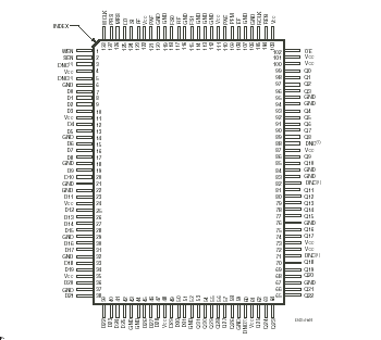
Pinout

  Connection Diagram


Specifications

Symbol
Rating
Industrial
Unit
VTERM(2)
Terminal Voltage with respect to GND
0.5 to +4.5
V
TSTG
Storage Temperature
55 to +125
IOUT
DC Output Current
50 to +50
mA


NOTES:
1. Stresses greater than those listed under ABSOLUTE MAXIMUM RATINGS may cause permanent
    damage to the device. This is a stress rating only and functional operation of the device at these
    or any other conditions above those indicated in the operational sections of this specification is not
    implied. Exposure to absolute maximum rating conditions for extended periods may affect reliability.
2. VCC terminal only.


Description

The IDT V-III and Vx-III Multimedia FIFOs of the IDT72V15160 are exceptionally deep, high speed, CMOS First-In-First-Out (FIFO) memories with independent clocked read and write controls and high density offerings up to 1 Mbit.

Each FIFO of the IDT72V15160 has a data input port (Dn) and a data output port (Qn). The frequencies of both the RCLK (read port clock) and the WCLK (write port clock) signals may vary from 0 to fS(MAX) with complete independence. There are no restrictions on the frequency of the one clock input with respect to the other.

These FIFOs of the IDT72V15160 have five flag pins, EF (Empty Flag), FF (Full Flag), HF (Halffull Flag), PAE (Programmable Almost-
Empty flag) and PAF (Programmable Almost-Full flag).

PAE and PAF can be programmed independently to switch at any point in memory. Programmable offsets determine the flag switching threshold and can be loaded with the serial interface to any user desired value or by default values. Eight default offset settings are provided, so that PAE can be set to switch at a predefined number of locations from the empty boundary and thePAF threshold can also be set at similar predefined values from the full boundary. The default offset values are set during Master Reset by the state of the FSEL0, FSEL1, and LD pins.

For serial programming of the IDT72V15160, SEN together with LD on each rising edge WCLK, are used to load the offset registers via the Serial Input (SI).

During Master Reset (MRS) the read and write pointers are set to the first location of the FIFO.


Customers Who Bought This Item Also Bought

Margin,quality,low-cost products with low minimum orders. Secure your online payments with SeekIC Buyer Protection.
Programmers, Development Systems
Semiconductor Modules
Power Supplies - Board Mount
Computers, Office - Components, Accessories
Power Supplies - External/Internal (Off-Board)
Prototyping Products
DE1
View more