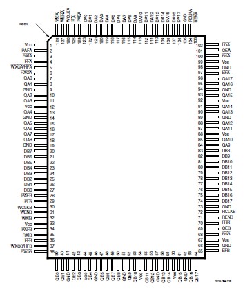
Features: • The IDT72805LB is equivalent to two IDT72205LB 256 x 18 FIFOs• The IDT72815LB is equivalent to two IDT72215LB 512 x 18 FIFOs• The IDT72825LB is equivalent to two IDT72225LB 1,024 x 18 FIFOs• The IDT72835LB is equivalent to two IDT72235LB 2,048 x 18 FIFOs• ...
IDT72845LB: Features: • The IDT72805LB is equivalent to two IDT72205LB 256 x 18 FIFOs• The IDT72815LB is equivalent to two IDT72215LB 512 x 18 FIFOs• The IDT72825LB is equivalent to two IDT722...
SeekIC Buyer Protection PLUS - newly updated for 2013!
268 Transactions
All payment methods are secure and covered by SeekIC Buyer Protection PLUS.
Symbol |
Rating |
Commercial &Industrial |
Unit |
VTERM |
Terminal Voltage with Respect to GND |
0.5 to +7.0 |
V |
TSTG |
Storage Temperature |
-55 to +125 |
oC |
IOUT |
DC Output Current |
-55 to +50 |
mA |
The IDT72845LB are dual 18-bit-wide synchronous (clocked) First-in, First-out (FIFO) memories. One dual IDT72805LB/ 72815LB/72825LB/72835LB/72845LB device is functionally equivalent to two IDT72205LB/72215LB/72225LB/72235LB/72245LB FIFOs in a single package with all associated control, data, and flag lines assigned to independent pins. These devices are very high-speed, low-power First-In, First-Out (FIFO) memories with clocked read and write controls. These FIFOs are applicable for a wide variety of data buffering needs, such as optical disk controllers, Local Area Networks (LANs), and interprocessor communication.
Each of the two FIFOs of the IDT72845LB contained in these devices has an 18-bit input and output port. Each input port is controlled by a free-running clock (WCLK), and an input enable pin (WEN). Data is read into the synchronous FIFO on every clock when WEN is asserted. The output port of each FIFO bank is controlled by another clock pin (RCLK) and another enable pin (REN). The Read Clock can be tied to the Write Clock for single clock operation or the two clocks can run asynchronous of one another for dual-clock operation. An Output Enable pin (OE) is provided on the read port of each FIFO for three-state control of the output.
The synchronous FIFOs of the IDT72845LB have two fixed flags, Empty Flag/Output Ready (EF/OR) and Full Flag/Input Ready (FF/IR), and two programmable flags, Almost-Empty (PAE) and Almost-Full (PAF). The offset loading of the programmableflags is controlled by a simple state machine, and is initiated by asserting the Load pin (LD). A Half-Full flag (HF) is available for each FIFO that is implemented as a single device configuration.
There are two possible timing modes of operation with these devices: IDT Standard mode and First Word Fall Through (FWFT) mode.
In IDT Standard Mode of the IDT72845LB, the first word written to an empty FIFO will not appear on the data output lines unless a specific read operation is performed. A read operation, which consists of activating REN and enabling a rising RCLK edge, will shift the word from internal memory to the data output lines.
In FWFT mode of the IDT72845LB, the first word written to an empty FIFO is clocked directly to the data output lines after three transitions of the RCLK signal. A REN does not have to be asserted for accessing the first word.
These devices of the IDT72845LB are depth expandable using a daisy-chain technique or First Word Fall Through (FWFT) mode. The XI and XO pins are used to expand the FIFOs. In depth expansion configuration, FL is grounded on the first device and set to HIGH for all other devices in the Daisy Chain.
The IDT72845LB are fabricated using IDT's high-speed submicron CMOS technology.