IDT723642

Features: • Free-running CLKA and CLKB may be asynchronous or coincident (simultaneous reading and writing of data on a single clock edge is permitted)• Two independent clocked FIFOs buffering data in opposite directions• Memory storage capacity: IDT723622256 x 36 x 2 IDT72363251...

product image

IDT723642 Picture
SeekIC No. : 004372420 Detail

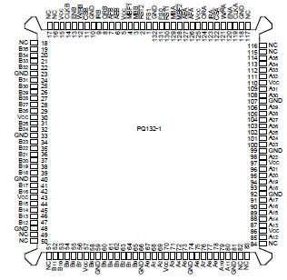
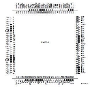
IDT723642: Features: • Free-running CLKA and CLKB may be asynchronous or coincident (simultaneous reading and writing of data on a single clock edge is permitted)• Two independent clocked FIFOs buf...

floor Price/Ceiling Price

Part Number:
IDT723642
Supply Ability:
5000

Price Break

  • Qty
  • 1~5000
  • Unit Price
  • Negotiable
  • Processing time
  • 15 Days
Total Cost: $ 0.00

SeekIC Buyer Protection PLUS - newly updated for 2013!

  • Escrow Protection.
  • Guaranteed refunds.
  • Secure payments.
  • Learn more >>

Month Sales

268 Transactions

Rating

evaluate  (4.8 stars)

Upload time: 2024/5/28

Payment Methods

All payment methods are secure and covered by SeekIC Buyer Protection PLUS.

Notice: When you place an order, your payment is made to SeekIC and not to your seller. SeekIC only pays the seller after confirming you have received your order. We will also never share your payment details with your seller.
Product Details

Description


Features:

• Free-running CLKA and CLKB may be asynchronous or coincident (simultaneous reading and writing of data on a
   single clock edge is permitted)
• Two independent clocked FIFOs buffering data in opposite directions
• Memory storage capacity: IDT723622256 x 36 x 2 IDT723632512 x 36 x 2 IDT7236421024 x 36 x 2
• Mailbox bypass register for each FIFO
• Programmable Almost-Full and Almost-Empty flags
• Microprocessor Interface Control Logic
• IRA, ORA, AEA, and AFA flags synchronized by CLKA
• IRB, ORB, AFA, and AFB flags synchronized by CLKB
• Supports clock frequencies up to 67MHz
• Fast access times of 11ns
• Available in 132-pin Plastic Quad Flatpack (PQF) or space-saving 120-pin Thin Quad Flatpack (PF)
• Low-power 0.8-Micron Advanced CMOS technology
• Industrial temperature range (-40oC to +85oC) is available, tested to military electrical specifications


Pinout

  Connection Diagram  Connection Diagram


Specifications

Symbol
Rating
Commercial
Unit
VCC
Supply Voltage Range
-0.5 to 7
V
VI(2)
Input Voltage Range
-0.5 to VCC+0.5
V
VO(2)
Output Voltage Range
-0.5 to VCC+0.5
V
IIK
Input Clamp Current, (VI < 0 or VI > VCC)
±20
mA
IOK
Output Clamp Current, (VO < 0 or VO > VCC)
±50
mA
IOUT
Continuous Output Current, (VO = 0 to VCC)
±50
mA
ICC
Continuous Current Through VCC or GND
±400
mA
TA
Operating Free Air Temperature Range
0 to 70
°C
TSTG
Storage Temperature Range
-65 to 150
°C
NOTES:
1. Stresses beyond those listed under "Absolute Maximum Ratings" may cause permanent
damage to the device. These are stress ratings only and functional operation of the device
at these or any other conditions beyond those indicated under "recommended operating
conditions" is not implied. Exposure to absolute-maximum-rated conditions for extended
periods may affect device reliability.
2. The input and output voltage ratings may be exceeded provided the input and output
current ratings are observed.


Description

The IDT723642 is a monolithic, high-speed, low-power, CMOS Bidirectional SyncFIFO (clocked) memory which supports clock frequencies up to 67MHz and have read access times as fast as 11ns. Two independent 256/512/ 1024x36 dual-port SRAM FIFOs on board each chip buffer data in opposite directions. Each FIFO has flags to indicate empty and full conditions and two programable flags (almost Full and almost Empty) to indicate when a selected number of words is stored in memory. Communication between each port may bypass the FIFOs via two 36-bit mailbox registers. Each mailbox register has a flag to signal when new mail has been stored. Two or more devices may be used in parallel to create wider data paths.

The IDT723642 is a synchronous (clocked) FIFO, meaning each port employs a synchronous interface. All data transfers through a port are gated to the LOW-to- HIGH transition of a port clock by enable signals. The clocks for each port are independent of one another and can be asynchronous or coincident. The enables for each port are arranged to provide a simple bidirectional interface between microprocessors and/or buses with synchronous control. The Input Ready (IRA, IRB) and Almost-Full (AFA, AFB) flags of a FIFO are two-stage synchronized to the port clock that writes data into its array. The Output Ready (ORA, ORB) and Almost-Empty (AEA, AEB) flags of a FIFO are two-stage synchronized to the port clock that reads data from its array. Offset values for the Almost-Full and Almost-Empty flags of both FIFOs can be programmed from Port A.

The IDT723642 is characterized for operation from 0°C to 70°C.


Customers Who Bought This Item Also Bought

Margin,quality,low-cost products with low minimum orders. Secure your online payments with SeekIC Buyer Protection.
Computers, Office - Components, Accessories
Transformers
Static Control, ESD, Clean Room Products
Cables, Wires
Batteries, Chargers, Holders
Crystals and Oscillators
View more