Features: •Memory storage capacity:
IDT723626256 x 36 x 2
IDT723636512 x 36 x 2
IDT7236461,024 x 36 x 2
•Clock frequencies up to 83 MHz (8ns access time)
•Two independent FIFOs buffer data between one bidirectional
36-bit port and two unidirectional 18-bit ports (Port C receives
and Port B transmits)
•18-bit (word) and 9-bit (byte) bus sizing of 18 bits (word) on Ports B and C
•Select IDT Standard timing (using EFA, EFB, FFA, and FFC flag
functions) or First Word Fall Through Timing (using ORA, ORB,
IRA, and IRC flag functions)
•Programmable Almost-Empty and Almost-Full flags; each has
three default offsets (8, 16 and 64)
•Serial or parallel programming of partial flags
•Big- or Little-Endian format for word and byte bus sizes
•Master Reset clears data and configures FIFO, Partial Reset
clears data but retains configuration settings
•Mailbox bypass registers for each FIFO
•Free-running CLKA, CLKB and CLKC may be asynchronous or
coincident (simultaneous reading and writing of data on a single
clock edge is permitted)
•Auto power down minimizes power dissipation
•Available in a space-saving 128-pin Thin Quad Flatpack (TQFP)
•Industrial temperature range (40°C to +85°C) is available
Pinout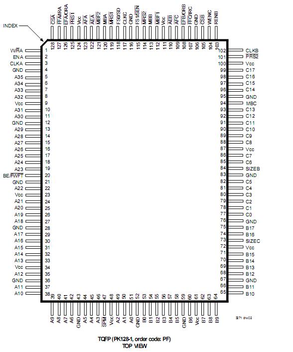 Specifications
|
Symbol |
Rating |
Commercial |
Unit |
|
VCC |
Supply Voltage Range |
0.5 to +7 |
V |
|
VI(2) |
Input Voltage Range |
0.5 to VCC+0.5 |
V |
|
VO(2) |
Output Voltage Range |
0.5 to VCC+0.5 |
V |
|
IIK |
Input Clamp Current (V < 0 or V > VCC) |
±20 |
mA |
|
IOK |
Output Clamp Current (VO= < 0 or VO> VCC) |
±50 |
mA |
|
IOUT |
Continuous Output Current (VO= 0 to VCC) |
±50 |
mA |
|
ICC |
Continuous Current Through VCC or GND |
±400 |
mA |
|
TSTG |
Storage Temperature Range |
65 to 150 |
°C |
DescriptionThe IDT723626 is a monolithic, high-speed, low-power, CMOS Triple Bus synchronous (clocked) FIFO memory which supports clock frequencies up to 83 MHz and has read access times as fast as8 ns. Two independent 256/512/1,024 x 36 dual-port SRAM FIFOs on board each chip buffer data between a bidirectional 36-bit bus (Port A) and two unidirectional 18-bit buses (Port B transmits data, Port C receives data.) FIFO data can be read out of Port B and written into Port C using either 18-bit or 9-bit formats with a choice of Big- or Little-Endian configurations.
These devices of the IDT723626 are a synchronous (clocked) FIFO, meaning each port employs a synchronous interface. All data transfers through a port are gated to the LOW-to-HIGH transition of a port clock by enable signals. The clocks for each port are independent of one another and can be asynchronous or coincident. The enables for each port are arranged to provide a simple

 IDT723626 Data Sheet