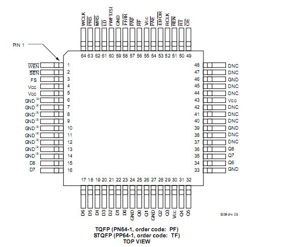
Features: • 16,384 x 9-bit storage capacity (IDT72261)
• 32,768 x 9-bit storage capacity (IDT72271)
• 10ns read/write cycle time (8ns access time)
• Retransmit Capability
• Auto power down reduces power consumption
• Master Reset clears entire FIFO, Partial Reset clears
data, but retains programmable settings
• Empty, Full and Half-full flags signal FIFO status
• Programmable Almost Empty and Almost Full flags, each
flag can default to one of two preselected offsets
• Program partial flags by either serial or parallel means
• Select IDT Standard timing (using ,EF and,FF flags) or
First Word Fall Through timing (using OR and IR flags)
• Easily expandable in depth and width
• Independent read and write clocks (permit simultaneous
reading and writing with one clock signal
• Available in the 64-pin Thin Quad Flat Pack (TQFP), 64-
pin Slim Thin Quad Flat Pack (STQFP) and the 68-pin
Pin Grid Array (PGA)
• Output enable puts data outputs into high impedance
• High-performance submicron CMOS technology
• Industrial temperature range (-40OC to +85OC) is avail-
able, tested to military electrical specificationsPinout Specifications
|
Symbol |
Rating |
Commercial |
MIilitary |
Unit |
|
VTERM |
Terminal Voltage with respect to GND |
0.5 to +7.0 |
0.5 to +7.0 |
V |
|
TA |
Operating
Temperature |
0 to +70 |
55 to +125 |
°C |
| TBIAS |
Temperature Under
Bias |
55 to +125 |
65 to +135 |
°C |
| TSTG |
Storage
Temperature |
55 to +125 |
65 to +155 |
°C |
| IOUT |
DC Output Current |
50 |
50 |
mA |
DescriptionThe IDT72271 are monolithic, CMOS, high capacity, high speed, low power first-in, first-out (FIFO) memories with clocked read and write controls. These FIFOs are applicable for a wide variety of data buffering needs, such as optical disk controllers, local area networks (LANs), and interprocessor communication.
Both FIFOs of the IDT72271 have a 9-bit input port (Dn) and a 9-bit output port (Qn). The input port is controlled by a free-running clock (WCLK) and a data input enable pin (,WEN ). Data is written into the synchronous FIFO on every clock when ,WEN is asserted. The output port is controlled by another clock pin
(RCLK) and enable pin (,REN). The read clock can be tied to the write clock for single clock operation or the two clocks can run asynchronously for dual clock operation. An output enable pin (,,OE ) is provided on the read port for three-state control of the outputs.
The IDT72271 have two modes of operation: In the IDT Standard Mode, the first word written to the FIFO is deposited into the memory array. A read operation is required to access that word. In the First Word Fall Through Mode (FWFT), the first word written to an empty FIFO appears automatically on the outputs, no read operation required. The state of the FWFT/SI pin during Master Reset determines the mode in use.
The IDT72271 FIFOs have five flag functions, ,EF/,OR(Empty Flag or Output Ready), ,EE/,IR (Full Flag or Input Ready), and HF (Half-full Flag). The ,EF and ,FF functions are selected in the IDT Standard Mode.
The ,IR and ,EFOR functions of the IDT72271 are selected in the First Word Fall Through Mode. ,IR indicates that the FIFO has free space to receive data. ,OR indicates that data contained in the FIFO is available for reading.
,EFHF of the IDT72271 is a flag whose threshold is fixed at the half-way point in memory. This flag can always be used irrespective of mode.
,PAE, ,PAF of the IDT72271 can be programmed independantly to any point in memory. They, also, can be used irrespective of mode. Programmable offsets determine the flag threshold and can be loaded by two methods: parallel or serial. Two default offset settings are also provided, such that ,PAE can be set at
127 or 1023 locations from the empty boundary and the ,PAF threshold can be set at 127 or 1023 locations from the full boundary. All these choices are made with,EFLD during Master Reset.
In the serial method, SEN together with LD are used to load the offset registers via the Serial Input (SI). In the parallel method, ,WEN together with ,LD can be used to load the offset registers via Dn. REN together with ,LD can be used to read the offsets in parallel from Qn regardless of whether serial or parallel offset loading is selected.
During Master Reset (,MRS) of the IDT72271 the read and write pointers are set to the first location of the FIFO. The FWFT line selects IDT Standard Mode or FWFT Mode. The ,LD pin selects one of two partial flag default settings (127 or 1023) and, also, serial or parallel programming. The flags are updated accordingly.
The Partial Reset ,(PRS) of the IDT72271 also sets the read and write pointers to the first location of the memory. However, the mode setting, programming method, and partial flag offsets are not altered. The flags are updated accordingly. ,PRS is useful for resetting a device in mid-operation, when reprogramming offset registers may not be convenient.

 IDT72271 Data Sheet


