IDT71V67602

Features: 256K x 36, 512K x 18 memory configurations Supports high system speed: 166MHz 3.5ns clock access time 150MHz 3.8ns clock access time 133MHz 4.2ns clock access time LBO input selects interleaved or linear burst modeSelf-timed write cycle with global write control (GW), byte write enable (...

product image

IDT71V67602 Picture
SeekIC No. : 004372341 Detail

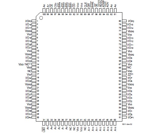
IDT71V67602: Features: 256K x 36, 512K x 18 memory configurations Supports high system speed: 166MHz 3.5ns clock access time 150MHz 3.8ns clock access time 133MHz 4.2ns clock access time LBO input selects interl...

floor Price/Ceiling Price

Part Number:
IDT71V67602
Supply Ability:
5000

Price Break

  • Qty
  • 1~5000
  • Unit Price
  • Negotiable
  • Processing time
  • 15 Days
Total Cost: $ 0.00

SeekIC Buyer Protection PLUS - newly updated for 2013!

  • Escrow Protection.
  • Guaranteed refunds.
  • Secure payments.
  • Learn more >>

Month Sales

268 Transactions

Rating

evaluate  (4.8 stars)

Upload time: 2024/6/10

Payment Methods

All payment methods are secure and covered by SeekIC Buyer Protection PLUS.

Notice: When you place an order, your payment is made to SeekIC and not to your seller. SeekIC only pays the seller after confirming you have received your order. We will also never share your payment details with your seller.
Product Details

Description


Features:

 256K x 36, 512K x 18 memory configurations
Supports high system speed:
166MHz 3.5ns clock access time
150MHz 3.8ns clock access time
133MHz 4.2ns clock access time
LBO input selects interleaved or linear burst mode
Self-timed write cycle with global write control (GW), byte write enable (BWE), and byte writes (BWx)
3.3V core power supply
Power down controlled by ZZ input
2.5V I/O supply (VDDQ)
Packaged in a JEDEC Standard 100-pin plastic thin quad flatpack (TQFP), 119 ball grid array (BGA) and 165 fine pitch ball grid array.


Pinout

  Connection Diagram


Specifications

Symbol Rating Commercial &
Industrial
Unit
VTERM(2) Terminal Voltage with
Respect to GND
-0.5 to +4.6 V
VTERM(3,6) Terminal Voltage with
Respect to GND
-0.5 to VDD V
VTERM(4,6) Terminal Voltage with
Respect to GND
-0.5 to VDD +0.5 V
VTERM(5,6) Terminal Voltage with
Respect to GND
-0.5 to VDDQ +0.5 V
TA(7) Commercial
Operating Temperature
-0 to +70 oC
Industrial
Operating Temperature
-40 to +85 oC
TBIAS Temperature
Under Bias
-55 to +125 oC
TSTG Storage
Temperature
-55 to +125 oC
PT Power Dissipation 2.0 W
IOUT DC Output Current 50 mA

NOTES:
1. Stresses greater than those listed under ABSOLUTE MAXIMUM RATINGS may cause permanent damage to the device. This is a stress rating only and functional operation of the device at these or any other conditions above those indicated in the operational sections of this specification is not implied. Exposure to absolute maximum rating conditions for extended periods may affect reliability.
2. VDD terminals only.
3. VDDQ terminals only.
4. Input terminals only.
5. I/O terminals only.
6. This is a steady-state DC parameter that applies after the power supplies have ramped up. Power supply sequencing is not necessary; however, the voltage on any input or I/O pin cannot exceed VDDQ during power supply ramp up.
7. TA is the "instant on" case temperature.


Description

The IDT71V67602/7802 are high-speed SRAMs organized as 256K x 36/512K x 18. The IDT71V676/78 SRAMs contain write, data, address and control registers. Internal logic allows the SRAM to generate a self-timed write based upon a decision which can be left until the end of the write cycle.

The burst mode feature offers the highest level of performance to the system designer, as the IDT71V67602/7802 can provide four cycles of data for a single address presented to the SRAM. An internal burst address counter accepts the first cycle address from the processor, initiating the access sequence. The first cycle of output data will be pipelined for one cycle before it is available on the next rising clock edge. If burst mode operation is selected (ADV=LOW), the subsequent three cycles of output data will be available to the user on the next three rising clock edges. The order of these three addresses are defined by the internal burst counter and theLBO input pin.

The IDT71V67602/7802 SRAMs utilize IDT's latest high-performance CMOS process and are packaged in a JEDEC standard 14mm x 20mm 100-pin thin plastic quad flatpack (TQFP) as well as a 119 ball grid array (BGA) and 165 fine pitch ball grid array (fBGA).


Customers Who Bought This Item Also Bought

Margin,quality,low-cost products with low minimum orders. Secure your online payments with SeekIC Buyer Protection.
LED Products
Power Supplies - External/Internal (Off-Board)
Isolators
Soldering, Desoldering, Rework Products
Optical Inspection Equipment
Inductors, Coils, Chokes
View more