Features: `128K x 36, 256K x 18 memory configurations
`Supports fast access times:
Commercial:
7.5ns up to 117MHz clock frequency
Commercial and Industrial:
8.0ns up to 100MHz clock frequency
8.5ns up to 87MHz clock frequency
`LBO input selects interleaved or linear burst mode
`Self-timed write cycle with global write control (GW), byte write
enable (BWE), and byte writes (BWx)
`3.3V core power supply
`Power down controlled by ZZ input
` 3.3V I/O
`Optional - Boundary Scan JTAG Interface (IEEE 1149.1 compliant)
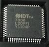
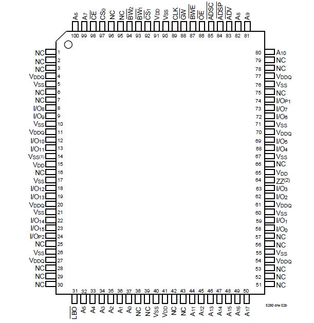
`Packaged in a JEDEC Standard 100-pin plastic thin quad flatpack (TQFP), 119 ball grid array (BGA) and 165 fine pitch ball grid arrayPinout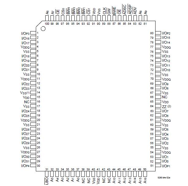
 Specifications
| Symbol |
Rating |
Commercial &
Industrial Values |
Unit |
| VTERM(2) |
Terminal Voltage with
Respect to GND |
-0.5 to +4.6 |
V |
| VTERM(3,6) |
Terminal Voltage with
Respect to GND |
-0.5 to VDD |
V |
| VTERM(4,6) |
Terminal Voltage with
Respect to GND |
-0.5 to VDD +0.5 |
V |
| VTERM(5,6) |
Terminal Voltage with
Respect to GND |
-0.5 to VDDQ +0.5 |
V |
| TA(7) |
Commercial
Operating Temperature |
-0 to +70 |
|
Industrial
Operating Temperature |
-40 to +85 |
|
| TBIAS |
Temperature
Under Bias |
-55 to +125 |
|
| TSTG |
Storage
Temperature |
-55 to +125 |
|
| PT |
Power Dissipation |
2.0 |
W |
| IOUT |
DC Output Current |
50 |
mA |
NOTES:
1. Stresses greater than those listed under ABSOLUTE MAXIMUM RATINGS may cause permanent damage to the device. This is a stress rating only and functional operation of the device at these or any other conditions above thosendicatedin the operational sections of this specification is not implied. Exposure to absolute maximum rating conditions for extended periods may affect reliability.
2. VDD terminals only.
3. VDDQ terminals only.
4. Input terminals only.
5. I/O terminals only.
6. This is a steady-state DC parameter that applies after the power supplies have ramped up. Power supplysequencing is not necessary; however, the voltage on any input or I/O pin cannot exceed VDDQ during power supply ramp up.
7. TA is the "instant on" case temperature.
DescriptionThe IDT71V3579S are high-speed SRAMs organized as 128K x 36/256K x 18. The IDT71V3579S SRAMs contain write, data, address and control registers. There are no registers in the data output path (flow-through architecture). Internal logic allows the SRAM to generate a self-timed write based upon a decision which can be left until the end of the write cycle.
The burst mode feature offers the highest level of performance to the system designer, as the IDT71V3579S can provide four cycles of data for a single address presented to the SRAM. An internal burst address counter accepts the first cycle address from the processor, initiating the access sequence. The first cycle of output data will flow-through from the array after a clock-to-data access time delay from the rising clock edge of the same cycle. If burst mode operation is selected (ADV=LOW), the subsequent three cycles of output data will be available to the user on the next three rising clock edges. The order of these three addresses are defined by the internal burst counter and theLBO input pin.
The IDT71V3579S SRAMs utilize IDT's latest high-performance CMOS process and are packaged in a JEDEC standard 14mm x 20mm 100-pin thin plastic quad flatpack (TQFP) as well as a 119 ball grid array (BGA) and a 165 fine pitch ball grid array (fBGA).

 IDT71V3579S Data Sheet