IDT71215

Features: • 16K x 15 Configuration 12 TAG Bits 3 Separate I/O Status Bits (Valid, Dirty, Write Through)• Match output uses Valid bit to qualify MATCH output• High-Speed Address-to-Match comparison times 8/9/10/12ns over commercial temperature range•BRDY circuitry include...

product image

IDT71215 Picture
SeekIC No. : 004372185 Detail

IDT71215: Features: • 16K x 15 Configuration 12 TAG Bits 3 Separate I/O Status Bits (Valid, Dirty, Write Through)• Match output uses Valid bit to qualify MATCH output• High-Speed Address-t...

floor Price/Ceiling Price

Part Number:
IDT71215
Supply Ability:
5000

Price Break

  • Qty
  • 1~5000
  • Unit Price
  • Negotiable
  • Processing time
  • 15 Days
Total Cost: $ 0.00

SeekIC Buyer Protection PLUS - newly updated for 2013!

  • Escrow Protection.
  • Guaranteed refunds.
  • Secure payments.
  • Learn more >>

Month Sales

268 Transactions

Rating

evaluate  (4.8 stars)

Upload time: 2024/7/15

Payment Methods

All payment methods are secure and covered by SeekIC Buyer Protection PLUS.

Notice: When you place an order, your payment is made to SeekIC and not to your seller. SeekIC only pays the seller after confirming you have received your order. We will also never share your payment details with your seller.
Product Details

Description


Features:

• 16K x 15 Configuration
   12 TAG Bits
   3 Separate I/O Status Bits (Valid, Dirty, Write Through)
• Match output uses Valid bit to qualify MATCH output
• High-Speed Address-to-Match comparison times
   8/9/10/12ns over commercial temperature range
•BRDY circuitry included inside the Cache-Tag for highest speed operation
• Asynchronous Read/Match operation with Synchronous Write and Reset operation
• Separate WE for the TAG bits and the Status bits
• Separate OE for the TAG bits, the Status bits, and BRDY
• Synchronous RESET pin for invalidation of all Tag entries
• Dual Chip selects for easy depth expansion with no performance degredation
• I/O pins both 5V TTL and 3.3V LVTTL compatible with VCCQ pins
•PWRDN pin to place device in low-power mode
• Packaged in a 80-pin Thin Plastic Quad Flat Pack (TQFP)


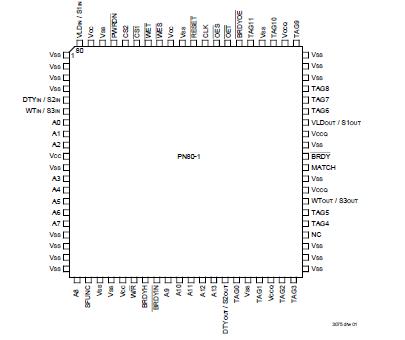
Pinout

  Connection Diagram


Specifications

Symbol
Rating
Value
Unit
VTERM
Terminal Voltage with Respect to GND
0.5 to +7.0(2)
V
TA
Operating Temperature
0 to +70
°C
TBIAS
Temperature Under Bias
65 to +135
°C
TSTG
Storage Temperature
65 to +150
°C
PT
Power Dissipation
1.7
W
IOUT
DC Output Current
20
mA
NOTES: 3075 tbl 08
1. Stresses greater than those listed under ABSOLUTE MAXIMUM RATINGS may cause permanent damage to the device. This is a stress rating only
   and   functional operation of the device at these or any other conditions above those indicated in the operational sections of this specification is
   not implied. Exposure to absolute maximum rating conditions for extended periods may affect reliabilty.
2. VIN should not exceed Vcc+0.5V. All pins should not exceed 7.0V. VCCQ should never exceed VCC, and VCC should never exceed VCCQ + 4.0V.


Description

This high-speed MATCH signal, with tADM as fast as 8ns, provides the fastest possible enabling of secondary cache accesses.

The three separate I/O status bits (VLD, DTY, and WT) of the IDT71215 can be configured for either dedicated or generic functionality, depending on the SFUNC input pin. With SFUNC LOW, the status bits are defined and used internally by the device, allowing easier determination of the validity and use of the given Tag data. SFUNC HIGH releases the defined internal status bit usage and control, allowing the user to configure the status bit information to fit his system needs. A synchronousRESET pin, when held LOW at a rising clock edge, will reset all status bits in the array for easy invalidation of all Tag addresses.

The IDT71215 also provides the option for Burst Ready (BRDY) generation within the cache tag itself, based upon MATCH, VLD bit, WT bit, and external inputs provided by the user. This can significantly simplify cache controller logic and minimize cache decision time. Match and Read operations are both asynchronous in order to provide the fastest access times possible, while Write operations are synchronous for ease of system timing.

The IDT71215 uses a 5V power supply on Vcc with separate VCCQ pins provided for the outputs to offer compliance with both 5.0V TTL and 3.3V LVTTL Logic levels. The PWRDN pin offers a low-power standby mode to reduce power consumption by 90%, providing significant system power savings.

The IDT71215 is fabricated using IDT's high-performance, high-reliability BiCMOS technology and is offered in a spacesaving 80-pin Thin Plastic Quad Flat Pack (TQFP) package.


Customers Who Bought This Item Also Bought

Margin,quality,low-cost products with low minimum orders. Secure your online payments with SeekIC Buyer Protection.
Cables, Wires
Isolators
Transformers
Optical Inspection Equipment
Discrete Semiconductor Products
Static Control, ESD, Clean Room Products
View more