IDT70V7589S

Features: ` 64K x 36 Synchronous Bank-Switchable Dual-ported SRAM Architecture 64 independent 1K x 36 banks- 2 megabits of memory on chip` Bank access controlled via bank address pins` High-speed data access -Commercial: 3.4ns (200MHz)/3.6ns (166MHz)/4.2ns (133MHz) (max.)-Industrial: 3.6ns (166MHz...

product image

IDT70V7589S Picture
SeekIC No. : 004372151 Detail

IDT70V7589S: Features: ` 64K x 36 Synchronous Bank-Switchable Dual-ported SRAM Architecture 64 independent 1K x 36 banks- 2 megabits of memory on chip` Bank access controlled via bank address pins` High-speed da...

floor Price/Ceiling Price

Part Number:
IDT70V7589S
Supply Ability:
5000

Price Break

  • Qty
  • 1~5000
  • Unit Price
  • Negotiable
  • Processing time
  • 15 Days
Total Cost: $ 0.00

SeekIC Buyer Protection PLUS - newly updated for 2013!

  • Escrow Protection.
  • Guaranteed refunds.
  • Secure payments.
  • Learn more >>

Month Sales

268 Transactions

Rating

evaluate  (4.8 stars)

Upload time: 2024/6/5

Payment Methods

All payment methods are secure and covered by SeekIC Buyer Protection PLUS.

Notice: When you place an order, your payment is made to SeekIC and not to your seller. SeekIC only pays the seller after confirming you have received your order. We will also never share your payment details with your seller.
Product Details

Description


Features:

` 64K x 36 Synchronous Bank-Switchable Dual-ported SRAM Architecture 64 independent 1K x 36 banks
   -  2 megabits of memory on chip
` Bank access controlled via bank address pins
` High-speed data access
   -Commercial: 3.4ns (200MHz)/3.6ns (166MHz)/4.2ns (133MHz) (max.)
   -Industrial: 3.6ns (166MHz)/4.2ns (133MHz) (max.)
` Selectable Pipelined or Flow-Through output mode
` Counter enable and repeat features
` Dual chip enables allow for depth expansion without additional logic
` Full synchronous operation on both ports
   -5ns cycle time, 200MHz operation (14Gbps bandwidth)
   -Fast 3.4ns clock to data out
   - 1.5ns setup to clock and 0.5ns hold on all control, data, and address inputs @ 200MHz
Data input, address, byte enable and control registers
Self-timed write allows fast cycle time
`Separate byte controls for multiplexed bus and bus matching compatibility
`LVTTL- compatible, 3.3V (±150mV) power supply for core
` LVTTL compatible, selectable 3.3V (±150mV) or 2.5V ±100mV)(±100mV) power supply for I/Os and control signals on
each port
` Industrial temperature range (-40°C to +85°C) is available at 166MHz and 133MHz
`Available in a 208-pin Plastic Quad Flatpack (PQFP),208-pin fine pitch Ball Grid Array (fpBGA), and 256-pin Ball
Grid Array (BGA)
` Supports JTAG features compliant with IEEE 1149.1


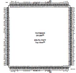
Pinout

  Connection Diagram


Specifications

Symbol Rating

Commercial
& Industrial
Unit
VTERM(2) Terminal Voltage with Respect to GND
-0.5 to +4.6
V
TBIAS Temperature Under Bias
55 to +125
TSTG Storage Temperature
65 to +150
IOUT DC Output Current
50
mA

NOTES:
1. Stresses greater than those listed under ABSOLUTE MAXIMUM RATINGS may cause permanent damage to the device. This is a stress rating only and functional operation of the device at these or any other conditions above those indicated in the operational sections of this specification is not implied. Exposure to absolute maximum rating conditions for extended periods may affect reliability.
2. VTERM must not exceed VDD + 150mV for more than 25% of the cycle time or4ns maximum, and is limited to  20mA for the period of VTERM VDD + 150mV.


Description

The IDT70V7589S is a high-speed 64Kx36 (2Mbit) synchronousBank-Switchable Dual-Ported SRAM organized into 64 independent1Kx36 banks. The device has two independent ports with separatecontrol, address, and I/O pins for each port, allowing each port to accessany 1Kx36 memory block not already accessed by the other port.Accesses by the ports into specific banks are controlled via the bankaddress pins under the user's direct control.

Registers of the IDT70V7589S on control, data, and address inputs provide minimal setupand hold times. The timing latitude provided by this approach allowssystems to be designed with very short cycle times. With an input data register, the IDT70V7589 has been optimized for applications havingunidirectional or bidirectional data flow in bursts. An automatic power downfeature, controlled by CE0 and CE1, permits the on-chip circuitry of eachport to enter a very low standby power mode. The dual chip enables alsofacilitate depth expansion.

The IDT70V7589S can support an operating voltage of either 3.3V or 2.5Von one or both ports, controllable by the OPT pins. The power supply forthe core of the device(VDD) remains at 3.3V. Please refer also to thefunctional description on page 19.


Customers Who Bought This Item Also Bought

Margin,quality,low-cost products with low minimum orders. Secure your online payments with SeekIC Buyer Protection.
Industrial Controls, Meters
Boxes, Enclosures, Racks
Hardware, Fasteners, Accessories
Memory Cards, Modules
View more