Features: 256K x 18 Synchronous Bank-Switchable Dual-ported
SRAM Architecture
64 independent 4K x 18 banks
4 megabits of memory on chip
Bank access controlled via bank address pins
High-speed data access
Commercial: 3.4ns (200MHz)/3.6ns (166MHz)/
4.2ns (133MHz) (max.)
Industrial: 3.6ns (166MHz)/4.2ns (133MHz) (max.)
Selectable Pipelined or Flow-Through output mode
Counter enable and repeat features
Dual chip enables allow for depth expansion without additional logic
Full synchronous operation on both ports
5ns cycle time, 200MHz operation (14Gbps bandwidth)
Fast 3.4ns clock to data out
1.5ns setup to clock and 0.5ns hold on all control, data, and address inputs @ 200MHz
Data input, address, byte enable and control registers
Self-timed write allows fast cycle time
Separate byte controls for multiplexed bus and bus matching compatibility
LVTTL- compatible, 3.3V (±150mV) power supply for core
LVTTL compatible, selectable 3.3V (±150mV) or 2.5V
(±100mV) power supply for I/Os and control signals on each port
Industrial temperature range (-40°C to +85°C) is available at 166MHz and 133MHz
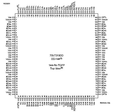
Available in a 144-pin Thin Quad Flatpack (TQFP),
208-pin fine pitch Ball Grid Array (fpBGA), and 256-pin Ball
Grid Array (BGA)
Supports JTAG features compliant with IEEE 1149.1
Due to limited pin count, JTAG is not supported on the
144-pin TQFP package.
Pinout Specifications
|
Symbol
|
Rating
|
Commercial
& Industrial |
Unit |
|
VTERM(2) |
Terminal Voltage
with Respect to
GND |
-0.5 to +4.6 |
V |
|
TBIAS |
Temperature
Under Bias |
-55 to +125 |
oC
|
|
TSTG |
Storage
Temperature |
-65 to +150 |
oC
|
|
IOUT |
DC Output Current |
50 |
mA |
DescriptionThe IDT70V7319S is a high-speed 256Kx18 (4Mbit) synchronous Bank-Switchable Dual-Ported SRAM organized into 64 independent 4Kx18 banks. The device has two independent ports with separate control, address, and I/O pins for each port, allowing each port to access any 4Kx18 memory block not alReady accessed by the other port. Accesses by the ports into specific banks are controlled via the bank address pins under the user's direct control.
Registers of the IDT70V7319S on control, data, and address inputs provide minimal setup and hold times. The timing latitude provided by this approach allows systems to be designed with very short cycle times. With an input data register, the IDT70V7319S has been optimized for applications having unidirectional or bidirectional data flow in bursts. An automatic power down feature, controlled by CE0 and CE1, permits the on-chip circuitry of each port to enter a very low standby power mode. The dual chip enables also facilitate depth expansion.
The IDT70V7319S can support an operating voltage of either 3.3V or 2.5V on one or both ports, controllable by the OPT pins. The power supply for the core of the device(VDD) remains at 3.3V. Please refer also to the functional description on page 19.

 IDT70V7319S Data Sheet


