Features: 32K x 16 Bank-Switchable Dual-Ported SRAM Architecture Four independent 8K x 16 banks 512 kilobit of memory on chip Fast asynchronous address-to-data access time: 15ns User-controlled input pins included for bank selects Independent port controls with asynchronous address & data bus...
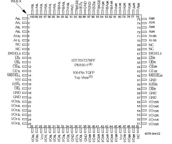
IDT70V7278S: Features: 32K x 16 Bank-Switchable Dual-Ported SRAM Architecture Four independent 8K x 16 banks 512 kilobit of memory on chip Fast asynchronous address-to-data access time: 15ns User-controlled inp...
SeekIC Buyer Protection PLUS - newly updated for 2013!
268 Transactions
All payment methods are secure and covered by SeekIC Buyer Protection PLUS.
Symbol |
Rating |
Commercial
& Industrial |
Unit |
VTERM |
Terminal Voltage with respect to GND |
-0.5 to +4.6 |
V |
VTER(2) |
Terminal Voltage |
-55 to +125 |
°C |
TSTG |
Temperature Under Bias |
-65 to +150
|
°C |
IOUT |
DC Output Current |
50
|
mA |
NOTES:
1. Stresses greater than those listed under ABSOLUTE MAXIMUM RATINGS may cause permanent damage to the device. This is a stress rating only and functional operation of the device at these or any other conditions above those indicated in the operational sections of this specification is not implied. Exposure to absolute maximum rating conditions for extended periods may affect reliability.
2. VTERM must not exceed Vcc + 5% for more than 25% of the cycle time or 10ns maximum, and is limited to < 20mA for the period of VTERM > Vcc + 5%.
The IDT70V7278S is a high-speed 32K x 16 (512K bit) Bank- Switchable Dual-Ported SRAM organized into four independent 8K 16 banks. The device has two independent ports with separate controls, addresses, and I/O pins for each port, allowing each port asynchronously access any 8K x 16 memory block not already accessed by the other port. Accesses by the ports into specific banks are controlled via bank select pin inputs under the user's control. Mailboxes are provided to allow inter-processor communications. Interrupts are provided to indicate mailbox writes have occurred.
An automatic power down feature of the IDT70V7278S controlled by the chip enables (CE0 and CE1) permits the on-chip circuitry of each port to enter a very low standby power mode and allows fast depth expansion. The IDT70V7278 offers a maximum address-to-data access time as fast as 15ns, and is packaged in a 100-pin Thin Quad Flatpack (TQFP).