IDT5V2305

Features: • High performance 1:5 clock driver for general purpose applications• Operates up to 170MHz at VDD = 2.5V• Operates up to 200MHz at VDD = 3.3V• Pin-to-pin skew < 50ps• VDD range: 2.3V to 3.6V• Output enable glitch suppression• 25 on-chip serie...

product image

IDT5V2305 Picture
SeekIC No. : 004371889 Detail

IDT5V2305: Features: • High performance 1:5 clock driver for general purpose applications• Operates up to 170MHz at VDD = 2.5V• Operates up to 200MHz at VDD = 3.3V• Pin-to-pin skew <...

floor Price/Ceiling Price

Part Number:
IDT5V2305
Supply Ability:
5000

Price Break

  • Qty
  • 1~5000
  • Unit Price
  • Negotiable
  • Processing time
  • 15 Days
Total Cost: $ 0.00

SeekIC Buyer Protection PLUS - newly updated for 2013!

  • Escrow Protection.
  • Guaranteed refunds.
  • Secure payments.
  • Learn more >>

Month Sales

268 Transactions

Rating

evaluate  (4.8 stars)

Upload time: 2024/8/14

Payment Methods

All payment methods are secure and covered by SeekIC Buyer Protection PLUS.

Notice: When you place an order, your payment is made to SeekIC and not to your seller. SeekIC only pays the seller after confirming you have received your order. We will also never share your payment details with your seller.
Product Details

Description


Features:

• High performance 1:5 clock driver for general purpose applications
• Operates up to 170MHz at VDD = 2.5V
• Operates up to 200MHz at VDD = 3.3V
• Pin-to-pin skew < 50ps
• VDD range: 2.3V to 3.6V
• Output enable glitch suppression
• 25 on-chip series dampening resistors
• Available in TSSOP and VFQFPN packages


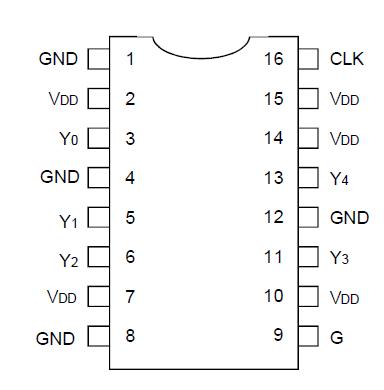
Pinout

  Connection Diagram


Specifications

Symbol Description
Max
Unit
VDD Power Supply Voltage
0.5 to +4.6
V
VI Input Voltage(2)
0.5 to VDD +0.5
V
VO Output Voltage(2)
0.5 to VDD +0.5
V
IIK VI < 0 or VI > VDD Input Clamp Current
±50
mA
IOK(VO < 0 or VO > VDD) Output Clamp Current
±50
mA
IO(VO < 0 to VDD) Continuous Output Current
±50
mA
TSTG Storage Temperature
65 to +165
°C

NOTES:
1. Stresses greater than those listed under ABSOLUTE MAXIMUM RATINGS may cause permanent damage to the device. This is a stress rating only and functional operation of the device at these or any other conditions above those indicated in the operational sections of this specification is not implied. Exposure to absolute maximum rating conditions for extended periods may affect reliability.
2. Not to exceed 4.6V.


Description

The IDT5V2305 is a high performance, low skew clock buffer that operates up to 200MHz. One bank of five outputs provides low skew copies of CLK. Through the use of control pin G, the outputs of bank Y(0:4) can be placed in a low state regardless of CLK input. The device operates in 2.5V and 3.3V environments. The built-in output enable glitch suppression ensures a synchronized output enable sequence to distribute full period clock signals.

The IDT5V2305 is characterized for operation from -40°C to +85°C.


Customers Who Bought This Item Also Bought

Margin,quality,low-cost products with low minimum orders. Secure your online payments with SeekIC Buyer Protection.
Soldering, Desoldering, Rework Products
Crystals and Oscillators
Prototyping Products
DE1
Cable Assemblies
Tapes, Adhesives
803
View more