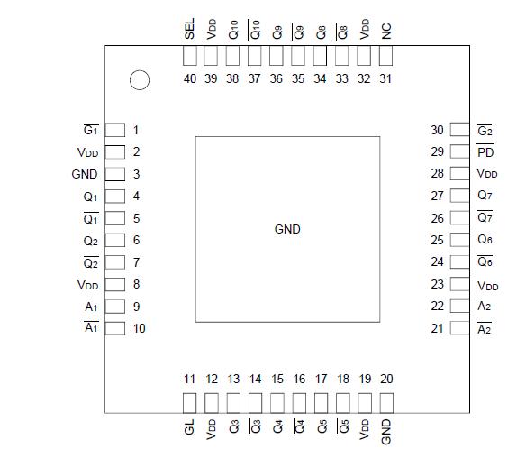
Features: • Guaranteed Low Skew < 25ps (max)• Very low duty cycle distortion < 125ps (max)• High speed propagation delay < 1.75ns (max)• Up to 1GHz operation• Selectable inputs• Hot insertable and over-voltage tolerant inputs• 3.3V / 2.5V LVTTL, H...
IDT5T9310: Features: • Guaranteed Low Skew < 25ps (max)• Very low duty cycle distortion < 125ps (max)• High speed propagation delay < 1.75ns (max)• Up to 1GHz operation• ...
SeekIC Buyer Protection PLUS - newly updated for 2013!
268 Transactions
All payment methods are secure and covered by SeekIC Buyer Protection PLUS.
Features: • IDT54/74FCT646 equivalent to FAST™speed;• IDT54/74FCT646A 30% faster...
Symbol | Description |
Max |
Unit |
VDD | Power Supply Voltage |
0.5 to +3.6 |
V |
VI | Input Voltage |
0.5 to +3.6 |
V |
VO | Output Voltage(2) |
0.5 to VDD +0.5 |
V |
TSTG | Storage Temperature |
65 to +150 |
°C |
TJ | Junction Temperature |
150 |
°C |
NOTES:
1. Stresses greater than those listed under ABSOLUTE MAXIMUM RATINGS may cause permanent damage to the device. This is a stress rating only and functional operation of the device at these or any other conditions above those indicated in the operational sections of this specification is not implied. Exposure to absolute maximum rating conditions for extended periods may affect reliability.
2. VDDQ and VDD internally operate independently. No power sequencing requirements need to be met.
3. Not to exceed 3.6V.
The IDT5T9310 2.5V differential clock buffer is a user-selectable differential input to ten LVDS outputs. The fanout from a differential input to ten LVDS outputs reduces loading on the preceding driver and provides an efficient clock distribution network. The IDT5T9310 can act as a translator from a differential HSTL, eHSTL, LVEPECL (2.5V), LVPECL (3.3V), CML, or LVDS input to LVDS outputs. A single-ended 3.3V / 2.5V LVTTL input can also be used to translate to LVDS outputs. The redundant input capability allows for an asynchronous change-over from a primary clock source to a secondary clock source. Selectable reference inputs are controlled by SEL.
The IDT5T9310 outputs can be asynchronously enabled/disabled. When disabled, the outputs will drive to the value selected by the GL pin. Multiple power and grounds reduce noise.