IDT5T2010

Features: • 2.5 VDD• 5 pairs of outputs• Low skew: 50ps same pair, 100ps all outputs• Selectable positive or negative edge synchronization• Tolerant of spread spectrum input clock• Synchronous output enable• Selectable inputs• Input frequency: 4.17MH...

product image

IDT5T2010 Picture
SeekIC No. : 004371872 Detail

IDT5T2010: Features: • 2.5 VDD• 5 pairs of outputs• Low skew: 50ps same pair, 100ps all outputs• Selectable positive or negative edge synchronization• Tolerant of spread spectrum ...

floor Price/Ceiling Price

Part Number:
IDT5T2010
Supply Ability:
5000

Price Break

  • Qty
  • 1~5000
  • Unit Price
  • Negotiable
  • Processing time
  • 15 Days
Total Cost: $ 0.00

SeekIC Buyer Protection PLUS - newly updated for 2013!

  • Escrow Protection.
  • Guaranteed refunds.
  • Secure payments.
  • Learn more >>

Month Sales

268 Transactions

Rating

evaluate  (4.8 stars)

Upload time: 2024/9/16

Payment Methods

All payment methods are secure and covered by SeekIC Buyer Protection PLUS.

Notice: When you place an order, your payment is made to SeekIC and not to your seller. SeekIC only pays the seller after confirming you have received your order. We will also never share your payment details with your seller.
Product Details

Description


Features:

• 2.5 VDD
• 5 pairs of outputs
• Low skew: 50ps same pair, 100ps all outputs
• Selectable positive or negative edge synchronization
• Tolerant of spread spectrum input clock
• Synchronous output enable
• Selectable inputs
• Input frequency: 4.17MHz to 250MHz
• Output frequency: 12.5MHz to 250MHz
• 1.8V / 2.5V LVTTL: up to 250MHz
• HSTL / eHSTL: up to 250MHz
• Hot insertable and over-voltage tolerant inputs
• 3-level inputs for selectable interface
• 3-level inputs for feedback divide selection with multiply ratios of(1-6, 8, 10, 12)
• Selectable HSTL, eHSTL, 1.8V/2.5V LVTTL, or LVEPECL input interface
• Selectable differential or single-ended inputs and ten singleended outputs
• PLL bypass for DC testing
• External differential feedback, internal loop filter
• Low Jitter: <75ps cycle-to-cycle
• Power-down mode
• Lock indicator
• Available in BGA and VFQFPN packages


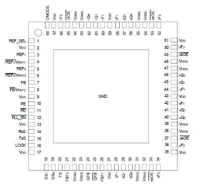
Pinout

  Connection Diagram


Specifications

Symbol Description
Max
Unit
VDD Power Supply Voltage(2)
0.5 to +3.6
V
VI Input Voltage
0.5 to +3.6
V
VO Output Voltage(3)
0.5 to VDDQ +0.5
V
VREF Reference Voltage(3)
0.5 to +3.6
V
TSTG Storage Temperature
65 to +165
°C
TJ Junction Temperature
150
°C

NOTES:
1. Stresses greater than those listed under ABSOLUTE MAXIMUM RATINGS may cause permanent damage to the device. This is a stress rating only and functional operation of the device at these or any other conditions above those indicated in the operational sections of this specification is not implied. Exposure to absolute maximum rating conditions for extended periods may affect reliability.
2. VDDQ and VDD internally operate independently. No power sequencing requirements need to be met.
3. Not to exceed 3.6V.


Description

The IDT5T2010 is a 2.5V PLL clock driver intended for high performance computing and data-communications applications. The IDT5T2010 has ten outputs in five banks of two, plus a dedicated differential feedback. The redundant input capability allows for a smooth change over to a secondary clock source when the primary clock source is absent.

The feedback bank allows divide-by-functionality from 1 to 12 through the use of the DS[1:0] inputs. This provides the user with frequency multiplication 1 to 12 without using divided outputs for feedback. Each output bank also allows for a divide-by functionality of 2 or 4.

The IDT5T2010 features a user-selectable, single-ended or differential input to ten single-ended outputs. The clock driver also acts as a translator from a differential HSTL, eHSTL, 1.8V/2.5V LVTTL, LVEPECL, or single-ended 1.8V/2.5V LVTTL input to HSTL, eHSTL, or 1.8V/2.5V LVTTL outputs. Selectable interface is controlled by 3-level input signals that may be hard-wired to appropriate high-mid-low levels. The outputs can be synchronously enabled/disabled.

Furthermore, when PE is held high, all the outputs are synchronized with the positive edge of the REF clock input. When PE is held low, all the outputs are synchronized with the negative edge of REF.


Customers Who Bought This Item Also Bought

Margin,quality,low-cost products with low minimum orders. Secure your online payments with SeekIC Buyer Protection.
Test Equipment
Tapes, Adhesives
803
Soldering, Desoldering, Rework Products
Crystals and Oscillators
Discrete Semiconductor Products
View more