IDT49FCT805PYB

Features: ·0.5 MICRON CMOS Technology·Guaranteed low skew < 700ps (max.)·Low duty cycle distortion < 1ns (max.)·Low CMOS power levels·TTL compatible inputs and outputs·Rail-to-rail output voltage swing·High drive: -24mA I OH, 64mA IOL·Two independent output banks with 3-state control·1:5 fan...

product image

IDT49FCT805PYB Picture
SeekIC No. : 004371698 Detail

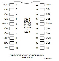
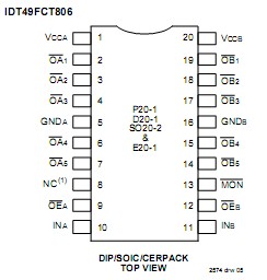
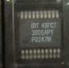
IDT49FCT805PYB: Features: ·0.5 MICRON CMOS Technology·Guaranteed low skew < 700ps (max.)·Low duty cycle distortion < 1ns (max.)·Low CMOS power levels·TTL compatible inputs and outputs·Rail-to-rail output volt...

floor Price/Ceiling Price

Part Number:
IDT49FCT805PYB
Supply Ability:
5000

Price Break

  • Qty
  • 1~5000
  • Unit Price
  • Negotiable
  • Processing time
  • 15 Days
Total Cost: $ 0.00

SeekIC Buyer Protection PLUS - newly updated for 2013!

  • Escrow Protection.
  • Guaranteed refunds.
  • Secure payments.
  • Learn more >>

Month Sales

268 Transactions

Rating

evaluate  (4.8 stars)

Upload time: 2025/3/14

Payment Methods

All payment methods are secure and covered by SeekIC Buyer Protection PLUS.

Notice: When you place an order, your payment is made to SeekIC and not to your seller. SeekIC only pays the seller after confirming you have received your order. We will also never share your payment details with your seller.
Product Details

Description


Features:

·0.5 MICRON CMOS Technology
·Guaranteed low skew < 700ps (max.)
·Low duty cycle distortion < 1ns (max.)
·Low CMOS power levels
·TTL compatible inputs and outputs
·Rail-to-rail output voltage swing
·High drive: -24mA I OH, 64mA IOL
·Two independent output banks with 3-state control
·1:5 fanout per bank
·"Heartbeat" monitor outp
·Available in DIP, SOIC, SSOP (805 only), QSOP (805 only), Cerpack and LCC packages
·Military product compliant to MIL-STD-883, Class B


Pinout

  Connection Diagram


  Connection Diagram


Specifications

Symbol Rating Max. Unit
VTERM(2) Terminal Voltagewith Respect to GND -0.5 to +7.0 V
VTERM(3) Terminal Voltagewith Respect to GND -0.5 to VCC +0.5 V
TSTG Storage Temperature -65 to +150
IOUT DC Output Current -60 to +120 mA

NOTES:                                                                                                         2574 lnk 03
1.Stresses greater than those listed under ABSOLUTE MAXIMUM RATINGS may cause permanent damage to the device.  This is a stress rating only and functional operation of the device at these or any other conditions above those indicated in the operational sections of this specification is not implied.  Exposure to absolute maximum rating conditions for extended periods may affect reliability.  No terminal voltage may exceed VCC by +0.5V unless otherwise noted.
2.Input and VCC terminals.
3.Output and I/O terminals.


Description

The IDT49FCT805PYB are clock drivers built using advanced dual metal CMOS technology. The IDT49FCT805/A is a non-inverting clock driver and the IDT49FCT806/A is an inverting clock driver. Each device consists of two banks of drivers. Each bank drives five output buffers from a standard TTL compatible  input.  The devices feature a "heartbeat" monitor for diagnostics and PLL driving.

The MON output of the IDT49FCT805PYB is identical to all other outputs and complies with the output specifications in this document.  The IDT49FCT805/A and IDT49FCT806/A offer low capacitance inputs with hysteresis.  Rail-to-rail output swing improves noise margin and allows easy interface with CMOS inputs.


Customers Who Bought This Item Also Bought

Margin,quality,low-cost products with low minimum orders. Secure your online payments with SeekIC Buyer Protection.
Cable Assemblies
Hardware, Fasteners, Accessories
LED Products
Programmers, Development Systems
Line Protection, Backups
Potentiometers, Variable Resistors
View more