ICS9DB202

Features: • Two 0.7V current mode differential HCSL output pairs• 1 differential clock input• CLK and nCLK supports the following input types: LVPECL, LVDS, LVHSTL, SSTL, HCSL• Maximum output frequency: 140MHz• Output skew: 110ps (maximum)• Cycle-to-cycle jitter...

product image

ICS9DB202 Picture
SeekIC No. : 004371353 Detail

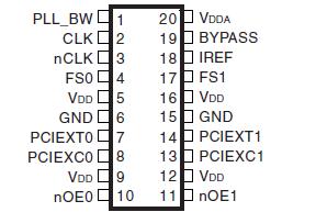
ICS9DB202: Features: • Two 0.7V current mode differential HCSL output pairs• 1 differential clock input• CLK and nCLK supports the following input types: LVPECL, LVDS, LVHSTL, SSTL, HCSL̶...

floor Price/Ceiling Price

Part Number:
ICS9DB202
Supply Ability:
5000

Price Break

  • Qty
  • 1~5000
  • Unit Price
  • Negotiable
  • Processing time
  • 15 Days
Total Cost: $ 0.00

SeekIC Buyer Protection PLUS - newly updated for 2013!

  • Escrow Protection.
  • Guaranteed refunds.
  • Secure payments.
  • Learn more >>

Month Sales

268 Transactions

Rating

evaluate  (4.8 stars)

Upload time: 2024/5/31

Payment Methods

All payment methods are secure and covered by SeekIC Buyer Protection PLUS.

Notice: When you place an order, your payment is made to SeekIC and not to your seller. SeekIC only pays the seller after confirming you have received your order. We will also never share your payment details with your seller.
Product Details

Description


Features:

• Two 0.7V current mode differential HCSL output pairs
• 1 differential clock input
• CLK and nCLK supports the following input types: LVPECL, LVDS, LVHSTL, SSTL, HCSL
• Maximum output frequency: 140MHz
• Output skew: 110ps (maximum)
• Cycle-to-cycle jitter: 110ps (maximum)
• RMS phase jitter @ 100MHz, (1.5MHz - 22MHz): 2.42ps (typical)
• 3.3V operating supply
• 0°C to 70°C ambient operating temperature
• Lead-Free package available
• Industrial temperature information available upon request


Pinout

  Connection Diagram


Specifications

Supply Voltage, VDD.......................... 4.6V
Inputs, VI .......................-0.5V to VDD + 0.5 V
Outputs, VO  ......................-0.5V to VDD + 0.5V
Package Thermal Impedance, JA
20 Lead TSSOP   .....................73.2°C/W (0 lfpm)
20 Lead SSOP ......................80.8°C/W (0 lfpm)
Storage Temperature, TSTG   ...............-65°C to 150°C
NOTE: Stresses beyond those listed under Absolute Maximum Ratings may cause permanent damage to the device. These ratings are stress specifications only. Functional operation of product at these conditions or any conditions beyond those listed in the DC Characteristics or AC Characteristics is not implied. Exposure to absolute maximum rating conditions for extended periods may affect product reliability.


Description

The ICS9DB202 is a high perfromance 1-to-2 Differential-to-HCSL Jitter Attenuator designed for use in PCI Express™ systems. In some PCI Express™ systems, such as those found in desktop PCs, the PCI Express™ clocks are generated from a low bandwidth, high phase noise PLL frequency synthesizer. In these systems, a jitter-attenuating device may be necessary in order to reduce high frequency random and deterministic jitter components from the PLL synthesizer and from the system board. The ICS9DB202 has two PLL bandwidth modes. In low bandwidth mode, the PLL loop bandwidth is 500kHz. This setting offers the best jitter attenuation and is still high enough to pass a triangular input spread spectrum profile. In high bandwidth mode, the PLL bandwidth is at 1MHz and allows the PLL to pass more spread spectrum modulation.

For serdes of the ICS9DB202 which have x10 reference multipliers instead of x12.5 multipliers, each of the two PCI Express™ outputs (PCIEX0:1) can be set for 125MHz instead of 100MHz by configuring the appropriate frequency select pins (FS0:1).


Customers Who Bought This Item Also Bought

Margin,quality,low-cost products with low minimum orders. Secure your online payments with SeekIC Buyer Protection.
Prototyping Products
DE1
Tapes, Adhesives
803
Optical Inspection Equipment
Semiconductor Modules
Crystals and Oscillators
View more