ICS9DB102

Features: • CLKREQ# pin for outputs 1 and 4/output enable for Express Card applications• PLL or bypass mode/PLL can dejitter incoming clock• Selectable PLL bandwidth/minimizes jitter peaking in downstream PLL's• Spread Spectrum Compatible/tracks spreading input clock for lo...

product image

ICS9DB102 Picture
SeekIC No. : 004371349 Detail

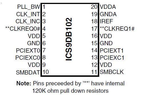
ICS9DB102: Features: • CLKREQ# pin for outputs 1 and 4/output enable for Express Card applications• PLL or bypass mode/PLL can dejitter incoming clock• Selectable PLL bandwidth/minimizes jitt...

floor Price/Ceiling Price

Part Number:
ICS9DB102
Supply Ability:
5000

Price Break

  • Qty
  • 1~5000
  • Unit Price
  • Negotiable
  • Processing time
  • 15 Days
Total Cost: $ 0.00

SeekIC Buyer Protection PLUS - newly updated for 2013!

  • Escrow Protection.
  • Guaranteed refunds.
  • Secure payments.
  • Learn more >>

Month Sales

268 Transactions

Rating

evaluate  (4.8 stars)

Upload time: 2024/5/31

Payment Methods

All payment methods are secure and covered by SeekIC Buyer Protection PLUS.

Notice: When you place an order, your payment is made to SeekIC and not to your seller. SeekIC only pays the seller after confirming you have received your order. We will also never share your payment details with your seller.
Product Details

Description


Features:

• CLKREQ# pin for outputs 1 and 4/output enable for Express Card applications
• PLL or bypass mode/PLL can dejitter incoming clock
• Selectable PLL bandwidth/minimizes jitter peaking in downstream PLL's
• Spread Spectrum Compatible/tracks spreading input clock for low EMI
• SMBus Interface/unused outputs can be disabled


Application

• 1-to-2 Zero-delay or fanout buffer for PCI Express


Pinout

  Connection Diagram


Specifications

Symbol
Parameter
Min
Max
Units
VDDA
3.3V Core Supply Voltage
VDD + 0.5V
V
VDD
3.3V Output Supply Voltage
GND - 0.5
VDD + 0.5V
V
Ts
Storage Temperature
-65
150
°C
Tambient
Ambient Operating Temp
0
70
°C
Tcase
Case Temperature
115
°C
ESD prot
Input ESD protection
human body model
2000
V


Description

The ICS9DB102 zero-delay buffer supports PCI Express clocking requirements. The ICS9DB102 is driven by a differential SRC output pair from an ICS K409/CK410-compliant main clock generator such as the ICS952601 or ICS954101. It attenuates jitter on the input clock and has a selectable PLL Band Width to maximize performance in systems with or without Spread-Spectrum clocking. An SMBus interface allows control of the PLL bandwidth and bypass options, while 2 clock request (OE#) pins make the ICS9DB102 suitable for Express Card applications.


Customers Who Bought This Item Also Bought

Margin,quality,low-cost products with low minimum orders. Secure your online payments with SeekIC Buyer Protection.
Prototyping Products
DE1
Connectors, Interconnects
Motors, Solenoids, Driver Boards/Modules
View more