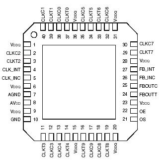
Features: • Low skew, low jitter PLL clock driver
• 1 to 10 differential clock distribution
• Feedback pins for input to output synchronization
• Spread Spectrum tolerant inputs
• Auto PD when input signal is at a certain logic state
• Available in 52-ball VFBGA and a 40-pin MLFApplication• DDR2 Memory Modules / Zero Delay Board Fan Out
• Provides complete DDR DIMM solution with IDT74SSTUAE32xxx familyPinout Specifications
| Item |
Rating |
Supply Voltage, (AVDD and VDDQ)
Logic Inputs
Ambient Operating Temperature
Storage Temperature |
-0.5V to 2.5V
GND - 0.5V to VDDQ + 0.5V
-40°C to +85°C
-65 to +150°C |
DescriptionThe PLL clock buffer, ICS98UAE877A, is designed for a VDDQ of 1.5V, an AVDD of 1.5V and differential data input and output levels.
ICS98UAE877A is a zero delay buffer that distributes a differential clock input pair (CLK_INT, CLK_INC) to ten differential pair of clock outputs (CLKT[0:9], CLKC[0:9]) and one differential pair feedback clock outputs (FB_OUTT, FBOUTC). The clock outputs are controlled by the input clocks (CLK_INT, CLK_INC), the feedback clocks (FB_INT, FB_INC), the LVCMOS program pins (OE, OS) and the Analog Power input (AVDD).
When OE of the ICS98UAE877A is low, the outputs (except FB_OUTT/FB_OUTC) are disabled while the internal PLL continues to maintain its locked-in frequency. OS (Output Select) is a program pin that must be tied to GND or VDDQ. When OS is high, OE will function as described above. When OS is low, OE has no effect on CLKT7/CLKC7 (they are free running in addition to FB_OUTT/FB_OUTC). When AVDD is grounded, the PLL is turned off and bypassed for test purposes. When both clock signals (CLK_INT, CLK_INC) are logic low, the ICS98UAE877A will enter a low power mode. An input logic detection circuit on the differential inputs, independent from the input buffers, will detect the logic low level and perform a low power state where all outputs, the feedback and the PLL are OFF. When the inputs transition from both being logic low to being differential signals, the PLL
will be turned back on, the inputs and outputs will be enabled and the PLL will obtain phase lock between the feedback clock pair (FB_INT, FB_INC) and the input clock pair (CLK_INT, CLK_INC) within the specified stabilization time tSTAB.
The PLL in ICS98UAE877A clock driver uses the input clocks (CLK_INT, CLK_INC) and the feedback clocks (FB_INT, FB_INC) to provide high-performance, low-skew, low-jitter output differential clocks (CLKT[0:9], CLKC[0:9]). ICS98UAE877A is also able to track Spread Spectrum Clocking (SSC) for reduced EMI. ICS98UAE877A is available in Commercial Temperature Range (0°C to 70°C) and Industrial Temperature Range (-40°C to +85°C). See Ordering Information for details

 ICS98UAE877A Data Sheet


