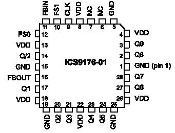
Features: • ICS9176-01-01 is pin compatible with Triquint GA1086• ±500ps skew (max) between input and outputs• ±250ps skew (max) between outputs• 10 symmetric, TLL-compatible outputs• 28-pin PLCC or 28-pin wide SOIC surface mount package• High drive, 40mA output...
ICS9176-01: Features: • ICS9176-01-01 is pin compatible with Triquint GA1086• ±500ps skew (max) between input and outputs• ±250ps skew (max) between outputs• 10 symmetric, TLL-compatible...
SeekIC Buyer Protection PLUS - newly updated for 2013!
268 Transactions
All payment methods are secure and covered by SeekIC Buyer Protection PLUS.
VDD referenced to GND . . . . . . . . . . . . . . . . . . . . . . . . . . . . . . . . . . 7V
Operating temperature under bias. . . . . . . . . . . . . . . . . 0°C to +70°C
Storage temperature . . . . . . . . . . . . . . . . . . . . . . . . -65°C to +150°C
Voltage on I/O pins referenced to GND. . . . . . .GND -0.5V to VDD +0.5V
Power dissipation . . . . . . . . . . . . . . . . . . . . . . . . . . . . . . . . . 0.5 Watts
Stresses above those listed under Absolute Maximum Ratings may cause permanent damage to the device. This is a stress rating only and functional operation of the device at these or any other conditions above those indicated in the operational sections of the specifications is not implied. Exposure to absolute maximum rating conditions for extended periods may affect product reliability.
the ICS9176-01 is designed specifically to support the tight timing requirements of high-performance microprocessors and chip sets. Because the jitter of the device is limited to ±250ps, the ICS9176-01 is ideal for clocking Pentium™ systems. The 10 high drive (40mA), low-skew (±250ps) outputs make the ICS9176-01 a perfect fit for PCI clocking requirements.
The ICS9176-01 has 10 outputs synchronized in phase and fre-quency to an input clock. The internal phase locked loop (PLL) acts either as a 1X clock multiplier or a 1/2X clock multiplier depending on the state of the input control pins T0 and T1. With metal mask options, any type of ratio between the input clock and output clock can be achieved, including 2X.
The PLL maintains the phase and frequency relationship between the input clock and the outputs by externally feeding back FBOUT to FBIN. Any change in the input will be tracked by all 10 outputs. However, the change at the outputs will happen smoothly so no glitches will be present on any driven input. The PLL circuitry matches rising edges of the input clock and the output clock. Since the input to FBIN skew is guaran-teed to ±500ps, the part acts as a "zero delay" buffer.
The ICS9176-01 has a total of eleven outputs. Of these, FBOUT is dedicated as the feedback into the PLL and another, Q/2, has an output frequency half that of the remaining nine. These nine outputs can either be running at the same speed as the input, or at half the frequency of the input. With Q/2 as the feedback to FBIN, the nine 'Q' outputs will be running at twice the input frequency in the normal divide-by-1 mode. In this case, the output can go to 120 MHz with a 60 MHz input clock.
The maximum rise and fall time of an output is 1ns and each is TTL-compatible with a 40mA symmetric drive.
The ICS9176-01 is fabricated using CMOS technology which results in much lower power consumption and cost compared with the gallium arsenide based 1086E. The typical operating current for the ICS9176-01 is 60mA versus 115mA for the GA1086E.