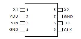
Features: • Ideal for set-top box applications using 13.5 MHz external pullable crystal to generate lock 27 MHz clock transport video clock• On-chip VCXO with guaranteed pull range of ±110 ppm minimum• VCXO input tuning voltage 0 to 3.3 V• Packaged in 8-pin SOIC (150 mil wi...
ICS728: Features: • Ideal for set-top box applications using 13.5 MHz external pullable crystal to generate lock 27 MHz clock transport video clock• On-chip VCXO with guaranteed pull range of ±1...
SeekIC Buyer Protection PLUS - newly updated for 2013!
268 Transactions
All payment methods are secure and covered by SeekIC Buyer Protection PLUS.
Features: • Operating voltage of 3.3 V ±0.3 V• Packaged in 8-pin SOIC• Available...
Item | Rating |
Supply Voltage, VDD | 7 V |
All Inputs and Outputs | -0.5 V to VDD+0.5 V |
Storage Temperature | -65 to +150°C |
Soldering Temperature | 260°C |
Stresses above the ratings listed below can cause permanent damage to the ICS728. These ratings, which are standard values for ICS commercially rated parts, are stress ratings only. Functional operation of the device at these or any other conditions above those indicated in the operational sections of the specifications is not implied. Exposure to absolute maximum rating conditions for extended periods can affect product reliability. Electrical parameters are guaranteed only over the recommended operating temperature range.
The ICS728 combines the functions of a VCXO (Voltage Controlled Crystal Oscillator) and PLL (Phase Locked Loop) frequency doubler onto a single chip. Used in conjunction with an external pullable quartz crystal, this monolithic integrated circuit replaces more costly hybrid (canned) VCXO devices. The ICS728 is designed primarily for data and clock recovery applications within end products such as set-top box receivers.
The ICS728 exhibits a moderate VCXO gain of 110 ppm/V typical, when used with a high quality external pullable quartz crystal.
The frequency of the on-chip VCXO is adjusted by an external control voltage input into pin VIN. Because VIN is a high impedance input, it can be driven directly from an PWM RC integrator circuit. Frequency output increases with VIN voltage input. The usable range of VIN is 0 to 3.3 V.