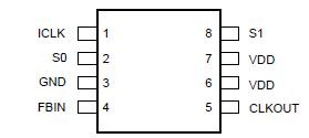
Features: • 8-pin MSOP package (3.00 mm x 3.00 mm body)• Available in Pb (lead) free package• Low input to output skew of 300 ps max• Can recover degraded input clock duty cycle• Output clock duty cycle of 45/55• Power Down and Tri-State Mode• Accepts spre...
ICS570-01: Features: • 8-pin MSOP package (3.00 mm x 3.00 mm body)• Available in Pb (lead) free package• Low input to output skew of 300 ps max• Can recover degraded input clock duty cy...
SeekIC Buyer Protection PLUS - newly updated for 2013!
268 Transactions
All payment methods are secure and covered by SeekIC Buyer Protection PLUS.
Stresses above the ratings listed below can cause permanent damage to the ICS570-01. These ratings, which are
standard values for IDT commercially rated parts, are stress ratings only. Functional operation of the device at these
or any other conditions above those indicated in the operational sections of the specifications is not implied.
Exposure to absolute maximum rating conditions for extended periods can affect product reliability. Electrical parameters are guaranteed only over the recommended operating temperature range.
Item | Rating |
Supply Voltage, VDD | 7V |
All Inputs and Outputs | -0.5 V to VDD+0.5 V |
Ambient Operating Temperature, Commercial version | 0 to +70 |
Ambient Operating Temperature, Industrial version | -40 to +85 |
Storage Temperature | -65 to +150 |
Junction Temperature | 125 |
Soldering Temperature | 260 |
The ICS570-01 is a high-performance Zero Delay Buffer (ZDB) which integrates IDT's proprietary mixed signal Phased Lock Loop (PLL) techniques. The zero delay feature means that the rising edge of the input clock aligns with the rising edges of the output clock, giving the appearance of no delay through the ICS570-01. The device includes an on-chip ROM table with nine different mulitplication factors, allowing it to generate many common output frequencies from a single input