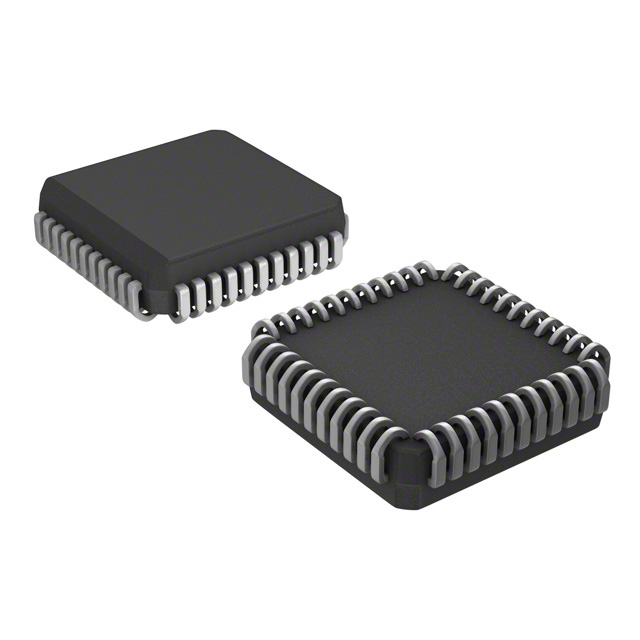
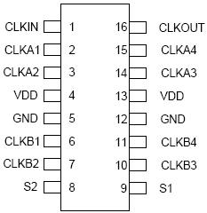
Features: • Clock outputs from 10 to 133 MHz• Zero input-output delay• Eight low skew (<250 ps) outputs• Device-to-device skew <700 ps• Full CMOS outputs with 25 mA output drive capability at TTL levels• 5 V tolerant CLKIN• Tri-state mode for board-l...
ICS2309: Features: • Clock outputs from 10 to 133 MHz• Zero input-output delay• Eight low skew (<250 ps) outputs• Device-to-device skew <700 ps• Full CMOS outputs with 25 ...
SeekIC Buyer Protection PLUS - newly updated for 2013!
268 Transactions
All payment methods are secure and covered by SeekIC Buyer Protection PLUS.
Item |
Rating |
Supply Voltage, VDD | 7 V |
All Inputs and Outputs | -0.5 V to VDD+0.5 V |
CLKIN and FBIN inputs | -0.5 V to 5.5 V |
Electrostatic Discharge (HBM) | 2000 V |
Ambient Operating Temperature (Commercial) | 0 to +70 |
Ambient Operating Temperature (Industrial) | -40 to +85 |
Storage Temperature | -65 to +150 |
Junction Temperature | 150 |
Soldering Temperature | 260 |
The ICS2309 is a low phase noise, high-speed PLL based, low-skew zero delay buffer. Based on ICS'proprietary low jitter Phase Locked Loop (PLL) techniques, the device provides eight low skew outputs at speeds up to 133 MHz at 3.3 V. The outputs can be generated from the PLL (for zero delay), or directly from the input (for testing), and can be set to tri-state mode or to stop at a low level. The PLL feedback is on-chip and is obtained from the CLKOUT pad.
The ICS2309 is available in two different versions. The ICS2309-1 is the base part. The ICS2309-1H is a high
drive version with faster rise and fall times.