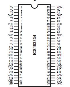
Features: • Meets JESD 82-2 specification• Internal series resistors to reduce switching noise• ±12 mA device capability• Low voltage operation- VDD = 3.3 ± 0.3V• 0.50 mm pitch, 56-Pin TSSOP packageApplication• PC133 Registered Memory Module• PC motherboar...
ICS162834: Features: • Meets JESD 82-2 specification• Internal series resistors to reduce switching noise• ±12 mA device capability• Low voltage operation- VDD = 3.3 ± 0.3V• 0.50 ...
SeekIC Buyer Protection PLUS - newly updated for 2013!
268 Transactions
All payment methods are secure and covered by SeekIC Buyer Protection PLUS.
The ICS162834 low voltage 18-bit register combines D-type latches and D-type flip-flops to allow data flow in transparent, latched and clocked modes. Date flow is controlled by output-enable (OE#), latch enable (LE#), and clock (CLK) inputs. The device operates in transparent mode when LE# is held low. The device operates in clocked mode when LE# is high and CLK is toggled. Data transfers from the inputs (A[18:1]) to outputs (Y[18:1]) on a positive edge transition of the clock. When OE# is low, the output state is enabled. When OE# is high, the output port is in a high impedance state.
The 18-bit registered buffer of the ICS162834 is designed to operate with a 3.0V to 4.6V supply voltage.
All inputs support operation with standard LVTTL interface levels. This includes data inputs, clock inputs and control inputs. Device outputs meet the requirements of the PC133 Registered DIMM specification. The device functions as defined supports latched, registered and flow through modes of operations. The PC133 Specification requires only registered mode.
Package of the ICS162834 is a 56 thin shrink small-outline package as defined by JEDEC Publication, JEP95, MO-153.