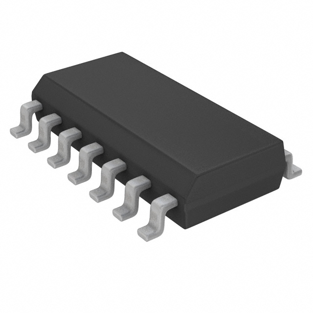
Pinout DescriptionThe I74F109D is designed as a dual positive edge-triggered JK-type flip-flop featuring individual J, K, clock, set, and reset inputs; also true and complementary outputs. Set (/SD) and reset (/RD) are asynchronous active low inputs and operate independently of the clock (CP) inp...
I74F109D: Pinout DescriptionThe I74F109D is designed as a dual positive edge-triggered JK-type flip-flop featuring individual J, K, clock, set, and reset inputs; also true and complementary outputs. Set (/SD...
SeekIC Buyer Protection PLUS - newly updated for 2013!
268 Transactions
All payment methods are secure and covered by SeekIC Buyer Protection PLUS.
The I74F109D is designed as a dual positive edge-triggered JK-type flip-flop featuring individual J, K, clock, set, and reset inputs; also true and complementary outputs. Set (/SD) and reset (/RD) are asynchronous active low inputs and operate independently of the clock (CP) input. The J and /K are edge-triggered inputs which control the state changes of the flip-flops as described in the function table. It has a feature that industrial temerature range available of -40°C to 85°C.
Some absolute maximum ratings of the I74F109D have been concluded into several points as follow. (1)Its supply voltage would be from -0.5V to 7.0V. (2)Its input voltage would be from -0.5V to 7.0V. (3)Its input current would be from -30mA to +5mA. (4)Its voltage applied to output in high output state would be from -0.5V to Vcc. (5)Its current applied to output in low output state would be 40mA. (6)Its operating free-air temperature range would be from 0°C to 70°C for commercial and would be from -40°C to 85°C for industrial. (7)Its storage temperature range would be from -65°C to 150°C. It should be noted that stresses above those listed in absolute maximum ratings may cause permanent damage to device.
Also some electrical characteristics of the I74F109D are concluded as follow. (1)Its high level output voltage would be min 2.5V and typ 3.4V. (2)Its low level output voltage would be typ 0.3V and max 0.5V. (3)Its input clamp voltage would be typ -0.73V and max -1.2V. (4)Its input current at maximum input voltage would be max 100uA. (5)Its high level input current would be max 20uA. (6)Its low level input current would be max -0.6mA for J, /K, CPn and would be max -1.8mA for /SDn, /RDn. (7)Its short circuit output current would be min -60mA and max -150mA. (8)Its supply current total would be typ 12.3mA and max 17mA. And so on. If you have any question or suggestion or want to know more information about the I74F109D please contact us for details. Thank you!