HY27UF082G2M

PinoutDescriptionThe HYNIX HY27UF082G2M series is a 256Mx8bit with spare 8Mx8 bit capacity. The device is offered in 3.3V Vcc Power Supply.HY27UF082G2M's NAND cell provides the most cost-effective solution for the solid state mass storage market.The memory is divided into blocks that can be erased...

product image

HY27UF082G2M Picture
SeekIC No. : 004368162 Detail

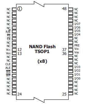
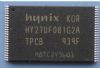
HY27UF082G2M: PinoutDescriptionThe HYNIX HY27UF082G2M series is a 256Mx8bit with spare 8Mx8 bit capacity. The device is offered in 3.3V Vcc Power Supply.HY27UF082G2M's NAND cell provides the most cost-effective s...

floor Price/Ceiling Price

Part Number:
HY27UF082G2M
Supply Ability:
5000

Price Break

  • Qty
  • 1~5000
  • Unit Price
  • Negotiable
  • Processing time
  • 15 Days
Total Cost: $ 0.00

SeekIC Buyer Protection PLUS - newly updated for 2013!

  • Escrow Protection.
  • Guaranteed refunds.
  • Secure payments.
  • Learn more >>

Month Sales

268 Transactions

Rating

evaluate  (4.8 stars)

Upload time: 2024/6/6

Payment Methods

All payment methods are secure and covered by SeekIC Buyer Protection PLUS.

Notice: When you place an order, your payment is made to SeekIC and not to your seller. SeekIC only pays the seller after confirming you have received your order. We will also never share your payment details with your seller.
Product Details

Description


Pinout

  Connection Diagram


Description

The HYNIX HY27UF082G2M series is a 256Mx8bit with spare 8Mx8 bit capacity. The device is offered in 3.3V Vcc Power Supply.

HY27UF082G2M's NAND cell provides the most cost-effective solution for the solid state mass storage market.
The memory is divided into blocks that can be erased independently so it is possible to preserve valid data while old data is erased.

The device HY27UF082G2M contains 2048 blocks, composed by 64 pages consisting in two NAND structures of 32 series connected Flash cells.
A program operation allows to write the 2112-byte page in typical 200us and an erase operation can be performed in typical 2ms on a 128K-byte(X8 device) block.

Data in the page mode can be read out at 50ns cycle time per byte. The I/O pins serve as the ports for address and data input/output as well as command input. This HY27UF082G2M interface allows a reduced pin count and easy migration towards different densities, without any rearrangement of footprint.

Commands, Data and Addresses are synchronously introduced using CE#, WE#, ALE and CLE input pin. The HY27UF082G2M on-chip Program/Erase Controller automates all program and erase functions including pulse repetition, where required, and internal verification and margining of data.

The modifying can be locked using the WP# input pin. The output pin RB# (open drain buffer) signals the status of the device HY27UF082G2M during each operation. In a system with multiple memories the RB# pins can be connected all together to provide a global status signal.

Even the write-intensive systems can take advantage of the HY27UF082G2M extended reliability of 100K program/ erase cycles by providing ECC (Error Correcting Code) with real time mapping-out algorithm.Optionally the chip could be offered with the CE# don't care function. This option allows the direct download of the code from the NAND Flash memory device by a microcontroller, since the CE# transitions do not stop the read operation.
The HY27UF082G2M copy back function allows the optimization of defective blocks management: when a page program operation fails
the data can be directly programmed in another page inside the same array section without the time consuming serial
data insertion phase.

The cache program feature allows the data insertion in the cache register while the data register is copied into the flash array. This pipelined program operation improves the program throughput when long files are written inside the memory HY27UF082G2M.
A cache read feature is also implemented. This HY27UF082G2M feature allows to dramatically improve the read throughput when consecutive pages have to be streamed out.

This device HY27UF082G2Mincludes also extra features like OTP/Unique ID area, Block Lock mechanism, Automatic Read at Power Up, Read ID2 extension.

The HYNIX HY27UF082G2Mseries is available in 48 - TSOP1 12 x 20 mm, 52-ULGA 12 x 17 mm.


Customers Who Bought This Item Also Bought

Margin,quality,low-cost products with low minimum orders. Secure your online payments with SeekIC Buyer Protection.
Prototyping Products
DE1
Semiconductor Modules
Memory Cards, Modules
Discrete Semiconductor Products
Cables, Wires
Boxes, Enclosures, Racks
View more