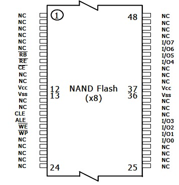
Features: HIGH DENSITY NAND FLASH MEMORIES- Cost effective solutions for mass storage applicationsNAND INTERFACE- x8 or x16 bus width.- Multiplexed Address/ Data- Pinout compatibility for all densitiesSUPPLY VOLTAGE- 3.3V device: VCC = 2.7 to 3.6V : HY27UAXX1G1M- 1.8V device: VCC = 1.7 to 1.95V : ...
HY27UA081G1M: Features: HIGH DENSITY NAND FLASH MEMORIES- Cost effective solutions for mass storage applicationsNAND INTERFACE- x8 or x16 bus width.- Multiplexed Address/ Data- Pinout compatibility for all densit...
SeekIC Buyer Protection PLUS - newly updated for 2013!
268 Transactions
All payment methods are secure and covered by SeekIC Buyer Protection PLUS.
Features: HIGH DENSITY NAND FLASH MEMORIES- Cost effective solutions for mass storage applications...
Symbol |
Parameter |
NAND Flash |
Unit | ||
Min |
Max | ||||
TBTAS |
Temperature Under Bias |
-50 |
125 |
||
TSTG |
Storage Temperature |
-65 |
150 |
||
VIO (1) |
Input or Output Voltage |
1.8V devices |
-0.6 |
2.7 |
V |
3.3 V devices |
-0.6 |
4.6 |
V | ||
VCC |
Supply Voltage |
1.8V devices |
-0.6 |
2.7 |
V |
3.3 V devices |
-0.6 |
4.6 |
V |
The HYNIX HY27UA081G1M series is a family of non-volatile Flash memories that use NAND cell technology. The devices operate 3.3V and 1.8V voltage supply. The size of a Page is either 528 Bytes (512 + 16 spare) or 264 Words (256 + 8 spare) depending on whether the device has a x8 or x16 bus width.
The HY27UA081G1M address lines are multiplexed with the Data Input/ Output signals on a multiplexed x8 or x16 Input/ Output bus.
This HY27UA081G1M interface reduces the pin count and makes it possible to migrate to other densities without changing the footprint. Each block can be programmed and erased over 100,000 cycles. To extend the lifetime of NAND Flash devices it is strongly recommended to implement an Error Correction Code (ECC). A Write Protect pin is available to give a hardware protection against program and erase operations.
The devices HY27UA081G1M feature an open-drain Ready/Busy output that can be used to identify if the Program/ Erase/Read (PER) Controller is currently active. The use of an open-drain output allows the Ready/ Busy pins from several memories to be connected to a single pull-up resistor.
A Copy Back command is available from HY27UA081G1M to optimize the management of defective blocks. When a Page Program operation fails, the data can be programmed in another page without having to resend the data to be programmed.
The devices HY27UA081G1M are available in the following packages:
- 48-TSOP1 (12 x 20 x 1.2 mm)
- 48-WSOP1 (12 x 17 x 0.7 mm)
- 63-FBGA (8.5 x 15 x 1.2 mm, 6 x 8 ball array, 0.8mm pitch)
Three options are available for the NAND Flash HY27UA081G1M family:
- Automatic Page 0 Read after Power-up, which allows the microcontroller to directly download the boot code from page 0.
- Chip Enable Dont Care, which allows code to be directly downloaded by a microcontroller, as Chip Enable transitions during the latency time do not stop the read operation.
- A Serial Number, which allows each device to be uniquely identified. The Serial Number options is subject to an NDA (Non Disclosure Agreement) and so not described in the datasheet. For more details of this option contact your nearest HYNIX Sales office.
Devices HY27UA081G1M are shipped from the factory with Block 0 always valid and the memory content bits, in valid blocks, erased to '1'.