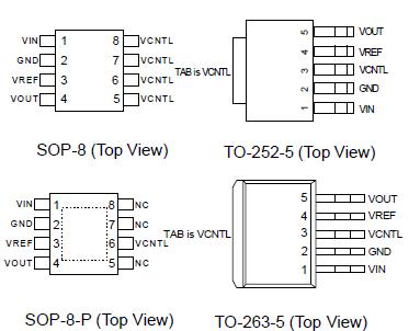
Features: • Provide Bi-direction Current- Sourcing or Sinking Current up to 3A• 1.25V/0.9V Output for DDR I/II Applications• Fast Transient Response• High Output Accuracy- ±20mV over Load, VOUT Offset and Temperature• Adjustable Output Voltage by External Resistors...
HPL5331: Features: • Provide Bi-direction Current- Sourcing or Sinking Current up to 3A• 1.25V/0.9V Output for DDR I/II Applications• Fast Transient Response• High Output Accuracy- ±2...
SeekIC Buyer Protection PLUS - newly updated for 2013!
268 Transactions
All payment methods are secure and covered by SeekIC Buyer Protection PLUS.
Symbol |
Parameter |
Rating |
Unit |
VCNTL |
VCNTL Supply Voltage, VCNTL to GND |
-0.2 ~ 7 |
V |
VIN |
VIN Supply Voltage, VIN to GND |
-0.2 ~ 3.9 |
V |
PD |
Power Dissipation |
Internally Limited |
W |
TJ |
Junction Temperature |
150 |
|
TSTG |
Storage Temperature |
-65 ~ 150 |
|
TSDR |
Soldering Temperature, 10 Seconds |
300 |
|
VESD |
Minimum ESD Rating (Human Body Mode) |
±3 |
kV |
The HPL5331 linear regulator is designed to provide a regulated voltage with bi-directional output current for DDR-SDRAM termination. It integrates two power transistors to source or sink current up to 3A. It also incorporate current-limit, thermal shutdown and shutdown control functions into a single chip. Current- limit circuit limits the short-circuit current.
On-chip thermal shutdown provides protection against any combination of overload that would create excessive junction temperature. The output voltage of HPL5331 track the voltage at VREF pin. A resistor divider connected to VIN, GND and VREF pins is used to provide a half voltage of VIN to VREF pin. In addition, an external ceramic capacitor and an opendrain transistor connected to VREF pin provides softstart and shutdown control respectively. Pulling and holding the VREF to GND shuts off the output. The output of HPL5331 will be high impedance after being shut down by VREF or thermal shutdown function.