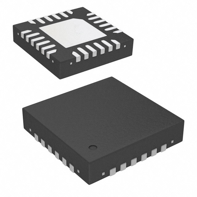
DescriptionThe HMC714LP5E is a dual-channel RMS power detector designed for high accuracy RF power signal measurement and control applications over the 0.1 to 3.9 GHz frequency range. The HMC714LP5 can be used with input signals having RMS values from -55 dBm to +15 dBm referenced to 50 and large crest factors with no accuracy degradation.
Each RMS detection channel is fully specified for operation up to 3.9 GHz, over a wide dynamic range of 70 dB. The HMC714LP5 operates from a single +5V supply and provides two linear-in-dB detection outputs at the RMSA and RMSB pins with scaled slopes of 37 mV/dB. The RMSA and RMSB channel outputs provide RMS detection performance in terms of dynamic range, logarithmic linearity and temperature stability similar to Hittite's HMC614LPE RMS Detector. The RMSA and RMSB outputs provide a read of average input signal power, or true-RMS power. Frequency detection up to 5.8 GHz is possible, with excellent channel matching of less than 0.5 dB (for the single-ended configuration), over a wide range of input frequencies with low temperature drift.
The HMC714LP5E also provides "channel difference" output ports via pins OUTP and OUTN, permitting measurements of the input signal power ratio between the two power detection channels. These outputs may be used in single-ended or differential configurations. An input voltage applied to the VLVL input pin is used to set the common mode voltage reference level for OUTP and OUTN. On the Hittite evaluation board, the VLVL pin is shorted to VREF2 output to provide a nominal bias voltage of 2.5V; but any external bias voltage may be used to set VLVL.
The HMC714LP5E also features INSA and INSB pins which provide a measurement of instantaneous signal power normalized to average power level in each channel. Reading both the INSA/INSB and RMSA/RMSB output voltage signals provides a very informative picture of the RF input signal; providing peak power, average power, peak-to-average power, and RF wave shape.
The device also includes a buffered PTAT temperature sensor output with a temperature scaling factor of 2.2 mV/°C yielding a typical output voltage of 600 mV at 0C. The HMC714LP5E operates over the -40 to +85C temperature range, and is available in a compact, 32-lead 5x5 mm leadless QFN package.

 HMC714LP5 / HMC714LP5E Data Sheet


