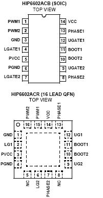
Features: • Drives Four N-channel MOSFETs
• Adaptive Shoot-Through Protection
• Internal Bootstrap Devices
• Supports High Switching Frequency
- Fast Output Rise Time
- Propagation Delay 30ns
• Small 14-Lead SOIC Package
• Smaller 16-Lead QFN Thermally Enhanced Package
• 5V to 12V Gate-Drive Voltages for Optimal Efficiency
• Three-State Input for Bridge Shutdown
• Supply Under-Voltage ProtectionApplication• Core Voltage Supplies for Intel Pentium® III and AMD® AthlonTM Microprocessors.
• High Frequency Low Profile DC/DC Converters
• High Current Low Voltage DC/DC ConvertersPinout SpecificationsSupply Voltage (VCC) ...........................................................15V
Supply Voltage (PVCC) ......................................................... VCC + 0.3V
BOOT Voltage (VBOOT - VPHASE) ..........................................15V
Input Voltage (VPWM) ...........................................................GND - 0.3V to 7V
UGATE.....................................................................................VPHASE - 0.3V to VBOOT + 0.3V
LGATE ....................................................................................GND - 0.3V to VPVCC + 0.3V
ESD Rating
Human Body Model (Per MIL-STD-883 Method 3015.7) ............3kV
Machine Model (Per EIAJ ED-4701 Method C-111) .....................200VDescriptionDesigned for versatility and speed, the HIP6602A two channel, dual MOSFET driver controls both high-side and low-side N-Channel FETs from two externally provided PWM signals.
The upper and lower gates of HIP6602A are held low until the driver is initialized. Once the VCC voltage surpasses the VCC Rising Threshold (See Electrical Specifications), the PWM signal takes control of gate transitions. A rising edge on PWM initiates the turn-off of the lower MOSFET (see Timing Diagram). After a short propagation delay [TPDL
LGATE], the lower gate begins to fall. Typical fall times [TF
LGATE] are provided in the Electrical Specifications section. Adaptive shoot-through circuitry monitors the LGATE voltage and determines the upper gate delay time [TPDHU
GATE] based on how quickly the LGATE voltage drops below 2.2V. This prevents both the lower and upper MOSFETs from conducting simultaneously or shoot-through. Once this delayperiod is complete the upper gate drive begins to rise [TR
UGATE] and the upper MOSFET turns on.

 HIP6602A Data Sheet


