HIP6502B

Features: •Provides 5 ACPI-Controlled Voltages-5VDUALUSB/Keyboard/Mouse (Active/Sleep)-3.3VDUAL/3.3VSBPCI/Auxiliary/LAN (Active/Sleep)-2.5VMEMRDRAM (Active/Sleep)-3.3VMEMSDRAM (Active/Sleep)-2.5VCLKClock/Processor Terminations (Active Only)•Excellent Output Voltage Regulation-3.3VDUAL/...

product image

HIP6502B Picture
SeekIC No. : 004362758 Detail

HIP6502B: Features: •Provides 5 ACPI-Controlled Voltages-5VDUALUSB/Keyboard/Mouse (Active/Sleep)-3.3VDUAL/3.3VSBPCI/Auxiliary/LAN (Active/Sleep)-2.5VMEMRDRAM (Active/Sleep)-3.3VMEMSDRAM (Active/Sleep)-2...

floor Price/Ceiling Price

Part Number:
HIP6502B
Supply Ability:
5000

Price Break

  • Qty
  • 1~5000
  • Unit Price
  • Negotiable
  • Processing time
  • 15 Days
Total Cost: $ 0.00

SeekIC Buyer Protection PLUS - newly updated for 2013!

  • Escrow Protection.
  • Guaranteed refunds.
  • Secure payments.
  • Learn more >>

Month Sales

268 Transactions

Rating

evaluate  (4.8 stars)

Upload time: 2024/10/31

Payment Methods

All payment methods are secure and covered by SeekIC Buyer Protection PLUS.

Notice: When you place an order, your payment is made to SeekIC and not to your seller. SeekIC only pays the seller after confirming you have received your order. We will also never share your payment details with your seller.
Product Details

Description


Features:

•Provides 5 ACPI-Controlled Voltages
-5VDUAL USB/Keyboard/Mouse (Active/Sleep)
-3.3VDUAL/3.3VSB PCI/Auxiliary/LAN (Active/Sleep)
-2.5VMEM RDRAM (Active/Sleep)
-3.3VMEM SDRAM (Active/Sleep)
-2.5VCLK Clock/Processor Terminations (Active Only)
•Excellent Output Voltage Regulation
-3.3VDUAL/3.3VSB Output:±2.0% Over Temperature;Sleep State Only
-2.5VMEM and 3.3VMEM Output:±2.0% Over
Temperature; Both Operational States (3.3VMEM in Sleep Only)
-2.5VCLK Output:±2.0% Over Temperature
•Small Size
-Very Low External Component Count
•Dual Memory Voltage Support Via MSEL Pin
-2.5V for RDRAM Memory
-3.3V for SDRAM Memory
-Both 2.5V and 3.3V for Flexible Systems
•Under-Voltage Monitoring of All Outputs with Centralized FAULT Reporting and Temperature Shutdown


Application

Motherboard Power Regulation for ACPI-Compliant Computers


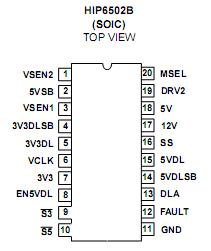
Pinout

  Connection Diagram


Specifications

Supply Voltage, V5VSB. . . . . . . . . . . . . . . . . . . . . . . . . . . . . .+7.0V
12V. . . . . . . . . . . . . . . . . . . . . . . . . . . . . .  . .GND - 0.3V to +14.5V
DLA, DRV2. . . . . . . . . . . . . . . . . . . . . . . .GND - 0.3V to V12V +0.3V
All Other Pins. . . . . . . . . . . . . . . . . . . . .GND - 0.3V to 5VSB + 0.3V
ESD Classification. . . . . . . . . . . . . . . . . . . . . . .  . . . . . . . . .Class 3


Description

The HIP6502B complements either an HIP6020 or an IP6021 in ACPI-compliant designs for microprocessor and omputer applications. The HIP6502B IC ntegrates four linear ontrollers/regulators, switching, monitoring and control unctions into a 20-pin SOIC package. One linear controller enerates the 3.3VDUAL /3.3VSB voltage plane from the ATX supply's 5VSB output, powering the south bridge and the PCI slots through an external pass transistor during sleep states (S3, S4/S5). A second transistor is used to switch in the ATX 3.3V output for operation during S0 and S1/S2 (active) operating states. Two linear controllers/regulators supply at choice either or both of the computer system's 2.5V or 3.3V memory power through external pass transistors in active states.

During sleep states, integrated pass transistors supply the sleep power for HIP6502B. Another controller powers up the 5VDUAL  plane by switching in the ATX 5V output in active states, and the ATX 5VSB in sleep states. One internal regulator outputs a dedicated, noise-free 2.5V clock chip supply. The HIP6502B's operating mode (active outputs or sleep outputs) is selectable through two digital control pins, S3 and S5. Enabling sleep state support on the 5VDUAL  output is offered through the EN5VDL pin. In active state, the 3.3VDUAL  and 3.3VMEM linear regulators use external N-channel pass MOSFETs to connect the outputs directly to the 3.3V input supplied by an ATX (or equivalent) power supply, for minimal losses. In sleep state, power delivery on both outputs is transferred to NPN transistors -external to the controller on the 3.3VDUAL , internal on the 3.3VMEM . Active state regulation on the 2.5VMEM   output is performed through an external NPN transistor. In sleep state, conduction on this output is transferred to an internal pass transistor. The 5VDUAL  output is powered through two external MOS transistors. In sleep states, a PMOS (or PNP) transistor conducts the current from the ATX 5VSB output; while in active state, current flow is transferred to an NMOS transistor connected to the ATX 5V output. The operation of the 5VDUALoutput is dictated not only by the status of the S3 and S5 pins, but that of the EN5VDL pin as well. The 3.3VDUAL /3.3VSB  output is active for as long as the ATX  5VSB voltage is applied to the chip. The 2.5VCLK  output is only active during S0 and S1/S2, and uses the 3V3 pin as input source for its internal pass element.


Customers Who Bought This Item Also Bought

Margin,quality,low-cost products with low minimum orders. Secure your online payments with SeekIC Buyer Protection.
Cables, Wires - Management
Power Supplies - Board Mount
LED Products
Cable Assemblies
View more