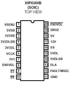
Features: • Provides 5 ACPI-Controlled Voltages
- 5V Active/Sleep (5VDUAL)
- 3.3V Active/Sleep (3.3VDUAL)
- 2.5V/3.3V Active/Sleep (2.5/3.3VMEM)
- 3.3V Always Present (3.3VSB)
- 2.5V Clock (Active Only) (2.5VCLK)
• Excellent Output Voltage Regulation
- 3.3VDUAL Output: ±2% Over Temperature; Sleep State Only
- 2.5V/3.3VMEM Output: ±2% Over Temperature; Both Operational States (3.3V setting in sleep only)
- 2.5VCLK and 3.3VSB Output: ±2% Over Temperature
• Small Size
- Very Low External Component Count
• Selectable Memory Output Voltage Via FAULT/MSEL Pin
- 2.5V for RDRAM Memory
- 3.3V for SDRAM Memory
• Under-Voltage Monitoring of All Outputs with Centralized FAULT Reporting and Temperature ShutdownApplication• Motherboard Power Regulation for ACPI-Compliant Computers Pinout SpecificationsSupply Voltage, V5VSB . . . . . . . . . . . . . . . . . . . . . . . . . . . . . +7.0V
12V. . . . . . . . . . . . . . . . . . . . . . . . . . . . . . . . GND - 0.3V to +14.5V
DLA, DRV2. . . . . . . . . . . . . . . . . . . . . . . .GND - 0.3V to V12V +0.3V
All Other Pins . . . . . . . . . . . . . . . . . . . . .GND - 0.3V to 5VSB + 0.3V
ESD Classification . . . . . . . . . . . . . . . . . . . . . . . . . . . . . . . . Class 3DescriptionThe HIP6500B complements either an HIP6020 or an HIP6021 in ACPI-compliant designs for microprocessor and computer applications. The HIP6500B IC integrates two linear controllers and two regulators, switching, monitoring and control functions into a 20-pin SOIC package. One linear controller generates the 3.3VDUAL voltage plane from the ATX supply's 5VSB output, powering the PCI slots through an external pass transistor during sleep states (S3, S4/S5). A second transistor is used to switch in the ATX 3.3V output for operation during S0 and S1/S2 (active) operating states. The second linear controller supplies the computer system's 2.5V/3.3V memory power through an external pass transistor in active states. During S3 state, an integrated pass transistor supplies the 2.5V/3.3V sleep power. A third controller powers up the 5VDUAL plane by switching in the ATX 5V output in active states, and the ATX 5VSB in sleep states. The two internal regulators consist of a low current 3.3V sleep output and a dedicated, noise-free 2.5V clock chip supply. The HIP6500B's operating mode (active outputs or sleep outputs) is selectable through two digital control pins, S3 and S5. Further control of the logic governing activation of different power states is offered through two configuration pins, EN3VDL and EN5VDL. In active state, the 3.3VDUAL linear regulator uses an external N-Channel pass MOSFET to connect the output directly to the 3.3V input supplied by an ATX (or equivalent) power supply, for minimal losses. In sleep state, power delivery on the 3.3VDUAL output is transferred to an NPN transistor, also external to the controller.
Active state power delivery for the 2.5/3.3VMEM output is performed through an external NPN transistor, or an NMOS switch for the 3.3V setting. In sleep state, conduction on this output of HIP6500B is transferred to an internal pass transistor. The 5VDUAL output is powered through two external MOS transistors. In sleep states, a PMOS (or PNP) transistor conducts the current from the ATX 5VSB output; while in active state, current flow is transferred to an NMOS transistor connected to the ATX 5V output. Similar to the 3.3VDUAL output, the operation of the 5VDUAL output is dictated not only by the status of the S3 and S5 pins, but that of the EN5VDL pin as well. The 3.3VSB internal regulator is active for as long as the ATX 5VSB voltage is applied to the chip, and derives its output current from the 5VSB pin. The 2.5VCLK output is only active during S0 and S1, and uses the 3V3 pin as input source for its internal pass element.

 HIP6500B Data Sheet


