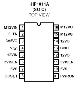
Features: • Adjustable Delay Time for Turn-Off and Fault Reporting
• Controls All PCI Supplies: +5V, +3.3V, +12V, -12V
• Internal MOSFET Switches for +12V and -12V Outputs
• µP Interface for On/Off Control and Fault Reporting
• Adjustable Overcurrent Protection for All Supplies
• Provides Fault Isolation
• Adjustable Turn-On Slew Rate
• Minimum Parts Count Solution
• No Charge PumpApplication• PCI Hot Plug
• CompactPCIPinout SpecificationsVCC, 12VIN . . . . . . . . . . . . . . . . . . . . . . . . . . . . . . . -0.5V to +14.0V
12VO . . . . . . . . . . . . . . . . . . . . . . . . . . . . . . -0.5V to V12VIN +0.5V
12VO, 12VG, 3V5VG . . . . . . . . . . . . . . . . . . . . . -0.5V to VCC +0.5V
M12VIN . . . . . . . . . . . . . . . . . . . . . . . . . . . . . . . . . . -15.0V to +0.5V
M12VO, M12VG. . . . . . . . . . . . . . . . . . . . . . VM12VIN-0.5V to +0.5V
3VISEN, 5VISEN . . . . . . . . . . . -0.5V to the Lesser of VCC or +7.0V
Voltage, Any Other Pin. . . . . . . . . . . . . . . . . . . . . . . . -0.5V to +7.0V
12VO Output Current . . . . . . . . . . . . . . . . . . . . . . . . . . . . .. . . . . .3A
M12VO Output Current . . . . . . . . . . . . . . . . . . . . . . . . . . . . . . . 0.8A
ESD Classification . . . . . . . . . . . . . . . . . . . . . . . . . . . .. ..4KeV (HBM)DescriptionThe HIP1011A is the second PCI Hot Plug Voltage bus control IC from Intersil. A drop-in alternative to the widely used HIP1011, the HIP1011A has the same form, fit and function but additionally features an adjustable latch-off time of the MOSFET switches and fault reporting.
Like the HIP1011, the HIP1011A creates a small and simple yet complete power control solution with discrete power MOSFETs and a few passive components. Four independent supplies are controlled, +5V, +3.3, +12V, and -12V. The +12V and -12V switches are integrated. For the +5V and +3.3V supplies, overcurrent (OC) protection is provided by sensing the voltage across external currentsense resistors. For the +12V and -12V supplies OC protection is provided internally. In addition, an on-chip reference is used to monitor the +5V, +3.3V and +12V outputs for undervoltage (UV) conditions. The PWRON input controls the state of the switches. During an OC condition on any output, or a UV condition on the +5V, +3.3V or +12V outputs, a LOW (0V) is asserted on the FLTN output and all MOSFETs are latched-off. The time to FLTN signal going LOW and MOSFET latch-off is determined by a single capacitor from the FLTN pin to ground. This added feature allows the system OS to complete housekeeping activities in preparation for an unplanned shut down of the affected card. The FLTN latch is cleared when the PWRON input is toggled low again. During initial power-up of the main VCC supply (+12V), the PWRON input is inhibited from turning on the switches, and the latch is held in the Reset state until the VCC input is greater than 10V.
User programmability of the overcurrent threshold, fault reporting response time, latch-off response time and turn-on slew rate is provided. A resistor connected to the OCSET pin programs the OC threshold. A capacitor may be added to the FLTN pin of HIP1011A to adjust both the delay time to reporting a fault and the latch-off of the supplies after an OC or UV event.
Capacitors connected to the gate pins set the turn-on rate. In addition the HIP1011A has also been enhanced to tolerate spurious system noise.

 HIP1011A Data Sheet


