HI3197

Features: • Resolution . . . . . . . . . . . . . . . . . . . . . . . . . . . . . . . 10 Bits• Conversion Rate 125 MSPS (PECL) 100 MSPS (TTL)• Data Input Level . . . . . . . . . . . . . . . . . . . . . . . . . . . . . .TTL• Low Power Consumption . . . . . . . . . . . . . . ....

product image

HI3197 Picture
SeekIC No. : 004362355 Detail

HI3197: Features: • Resolution . . . . . . . . . . . . . . . . . . . . . . . . . . . . . . . 10 Bits• Conversion Rate 125 MSPS (PECL) 100 MSPS (TTL)• Data Input Level . . . . . . . . . . ....

floor Price/Ceiling Price

Part Number:
HI3197
Supply Ability:
5000

Price Break

  • Qty
  • 1~5000
  • Unit Price
  • Negotiable
  • Processing time
  • 15 Days
Total Cost: $ 0.00

SeekIC Buyer Protection PLUS - newly updated for 2013!

  • Escrow Protection.
  • Guaranteed refunds.
  • Secure payments.
  • Learn more >>

Month Sales

268 Transactions

Rating

evaluate  (4.8 stars)

Upload time: 2024/12/25

Payment Methods

All payment methods are secure and covered by SeekIC Buyer Protection PLUS.

Notice: When you place an order, your payment is made to SeekIC and not to your seller. SeekIC only pays the seller after confirming you have received your order. We will also never share your payment details with your seller.
Product Details

Description


Features:

• Resolution . . . . . . . . . . . . . . . . . . . . . . . . . . . . . . . 10 Bits
• Conversion Rate 125 MSPS (PECL) 100 MSPS (TTL)
• Data Input Level . . . . . . . . . . . . . . . . . . . . . . . . . . . . . .TTL
• Low Power Consumption . . . . . . . . . . . . . . . 400mW (Typ)
• Low Glitch Energy . . . . . . . . . . . . . . . . . . . . . . . . 1.5pV•s
• Clock, Reset Input Level: TTL and PECL Compatible 2:1 Multiplexed Input Function
• 1/2 Frequency-Divided Clock Output Possible by the Built- In Clock Frequency Divider Circuit
• Voltage Output (50Ω Load Drive Possible)
• Single Power Supply or ±Dual Power Supplies
• Polarity Switching Function of Reset Signal


Application

• LCD
• DDS
• HDTV
• Communications (QPSK, QAM)


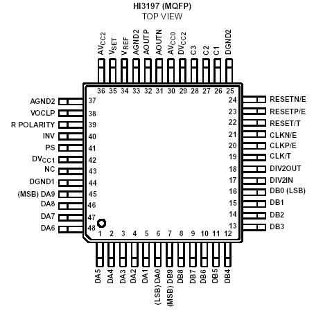
Pinout

  Connection Diagram


Specifications

Supply Voltage (AVCC0, AVCC2, DVCC2) . . . . . . . . . . . -0.5 to +7.0V
AGND2, DGND2 . . . . . . . . . . . . . . . . . . . . . . . . . . .. . . -7.0 to +0.5V
DVCC1 . . . . . . . . . . . . . . . . . . . . . . . . . . . . . . . . . ..  . -0.5 to +7.0V
AVCC2 - AGND2. . . . . . . . . . . . . . . . . . . . . . . . . . .. . . -0.5 to +7.0V
AVCC0 - AGND2. . . . . . . . . . . . . . . . . . . . . . . . . .. . . . -0.5 to +7.0V
DVCC2 - DGND2 . . . . . . . . . . . . . . . . . . . . . . . . .. . . . -0.5 to +7.0V
Input Voltage
VSET, . . . . . . . . . . . . . . . . . . . . . . . .. .AGND2 -05 to AVCC2 + 0.5V
TTL Pin . . . . . . . . . . . . . . . . . . . . .. . . DGND1 -0.5 to DVCC1 + 0.5V
PECL Pin, . . . . . . . . . . . . . . . . . .. . . . DGND1 -0.5 to DVCC1 + 0.5V
PS. . . . . . . . . . . . . . . . . . . . . . . . . . . DGND1 -0.5 to DVCC1 + 0.5V
(Others), VOCLP . . . . . . . . . . . . . . . . . DGND1 -0.5 to DVCC1 + 5V


Description

The HI3197 is a high-speed D/A converter which can perform the multiplexed input of the two system 10-bit data.

The maximum conversion rate of HI3197 achieves 125 MSPS. The multiplexed operation is possible by the 1/2 frequencydivided clock or by halving the frequency of the clock with the clock frequency divider circuit having the reset pin in the IC. The data input is TTL; the clock input pin and reset input pin can select either TTL or PECL according to the application.


Customers Who Bought This Item Also Bought

Margin,quality,low-cost products with low minimum orders. Secure your online payments with SeekIC Buyer Protection.
Resistors
Optical Inspection Equipment
Cables, Wires - Management
Line Protection, Backups
Circuit Protection
View more