Features: ·Fully DVB&DSS compliant
·Dual 6bit A/D converters
·Continuously variable symbol rate from 1Msps to 55Msps (75MHz clock)
·Internal digital root raised cosine filter
·Less than 0.5 dB implementation loss
·Frequency multiplexing capability
·Automated frequency search
·Internal bias cancellation
·Both wideband and narrowband AGC
·Noise calibration for antenna steering
·Output data rate as high as 68Mbps
·Fixed frequency sampling clock
·Simple interface with tuner and analog processing
·Microcontroller interface
·Eight bit parallel or I2C monitor and control interface
·I2C by-pass mode
·Two package typesPinout Specifications
| Rating |
Value |
Unit |
| Ambient Temperature under Bias |
-10 to 70 |
c |
| Storage Temperature |
-65 to 150 |
c |
| Ambient Humidity under Bias |
85(85 c,500hrs) |
% |
| Thermal Resistance(Ja) |
45 |
c/W |
| Junction Temperature |
150 |
c |
| Voltage on Any Pin |
Vss - 0.3V to VDD + 0.5V |
V |
| VDD, IOVDD |
5.5 |
V |
| Package Material |
- Compound : CEL-4630SX
- Lead Frame : Copper |
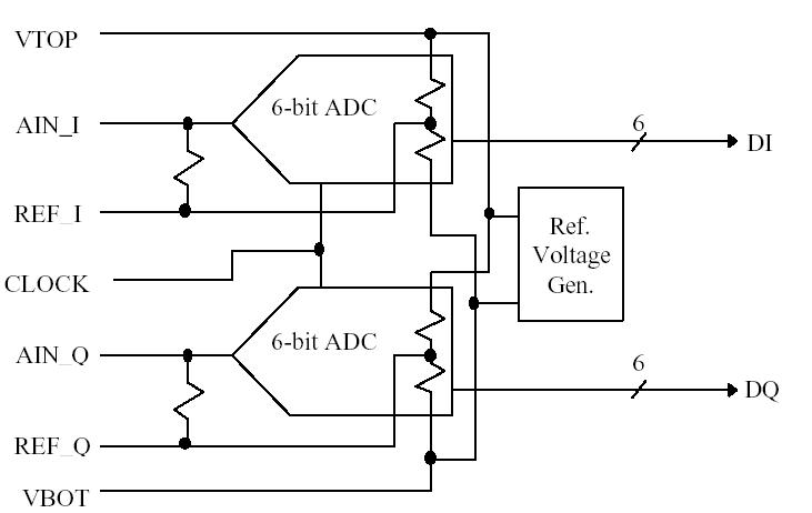
DescriptionThe HDM8513A digital demodulator for direct broadcast satellite receivers is a single chip solution fully compliant with the European Telecommunications Standards Institute (ETSI) specification ETS 300 421. This chip integrates an A/D converter, a variable rate matched filter, a variable rate QPSK demodulator with a Viterbi decoder, a deinterleaver and a Reed Solomon decoder.
The HDM8513A, which is implemented in a 0.35 micron CMOS, Triple Layer Metal Process, provides variable rate capability while operating with a fixed frequency sampling clock. Digital samples of baseband I and Q data are generated by an internal A/D converter, then provided to the demodulator at a fixed sample rate. The root raised cosine filter is implemented internally with fully digital techniques. Similarly, the symbol timing recovery and carrier phase tracking functions are performed entirely in the digital domain. This approach provides minimum constraints on external circuits, thus reducing overall system costs.
The HDM8513A may be configured by an external processor for a specific symbol rate, and carrier frequency along with loop gain parameters. The HDM8513A provides an external AGC signal which is used to control the gain of the analog signal which is applied to the down-converters. And it also provides a digital AGC internally which controls the gain of the signal out of the matched filters. In addition, the HDM8513A provides fully programmable sweep circuitry to aid in initial acquisition when large frequency offsets may be present.
The digital frequency translation capability of the HDM8513A permits this part to be used in frequency multiplexing applications. In this application, an entire transponder bandwidth containing many signals is sampled at a fixed rate. The digital oscillator within the HDM8513A is programmed to the specific desired carrier frequency within that band to permit the selected signal to be passed through the baseband filter and processed by the demodulator circuits.

 HDM8513A Data Sheet


