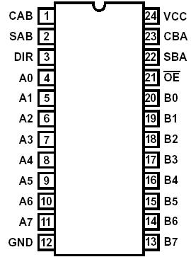
Features: • 3 Micron Radiation Hardened CMOS SOS• Total Dose 200K RAD (Si)• SEP Effective LET No Upsets: >100 MEV-cm2/mg• Single Event Upset (SEU) Immunity < 2 x 10⁻⁹ Errors/ Bit-Day (Typ)• Dose Rate Survivability: >1 x 10¹² RAD (Si)/s• Dose Rate Upset ...
HCTS646MS: Features: • 3 Micron Radiation Hardened CMOS SOS• Total Dose 200K RAD (Si)• SEP Effective LET No Upsets: >100 MEV-cm2/mg• Single Event Upset (SEU) Immunity < 2 x 10⁻⁹ E...
SeekIC Buyer Protection PLUS - newly updated for 2013!
268 Transactions
All payment methods are secure and covered by SeekIC Buyer Protection PLUS.
Supply Voltage (VCC). . . . . . . . . . . . . . . . . . . . . . -0.5V to +7.0V
Input Voltage Range, All Inputs . . . . . . . . . . .-0.5V to VCC +0.5V
DC Input Current, Any One Input . . . . . . . . . . . . . . . . . ..±10mA
DC Drain Current, Any One Output. . . . . . . . . . . . . . . . . .±25mA
(All Voltage Reference to the VSS Terminal)
Storage Temperature Range (TSTG) . . . . . . . . . . -65 to +150
Lead Temperature (Soldering 10sec) . . . . . . . . . . . . . . . . +265
Junction Temperature (TJ) . . . . . . . . . . . . . . . . . . . . . . . . .+175
ESD Classification . . . . . . . . . . . . . . . . . . . . . . . . . . . . . . . Class 1
CAUTION: As with all semiconductors, stress listed under "Absolute Maximum Ratings" may be applied to devices (one at a time) without resulting in permanent damage. This is a stress rating only. Exposure to absolute maximum rating conditions for extended periods may affect device reliability. The conditions listed under "Electrical Performance Characteristics" are the only conditions recommended for satisfactory device operation.
The Intersil HCTS646MS is a Radiation Hardened Three- State Octal Bus Tranceiver/Register with Non-Inverting outputs. This HCTS646MS is a bus transceiver with D-type flip-flops which act as internal storage registers. Data on the A bus or the B bus can be clocked into the registers on a High-to-Low transition of either CAB ro CBA clock inputs. Output enable (OE) and Direction (DIR) inputs control the transceiver functions.
Data present at the high impedance output can be stored in either register or both but only one of the two buses can be enabled as outputs at any one time. The select controls (SAB and SBA) can multiplex stored and transparent (real time) data. The direction control of HCTS646MS determines which data bus will receive data when the OE pin is LOW. In the high impedance mode (OE high), A data can be stored in one register and B data in the other register. Data at the A or B terminals can be clocked into the storage flip-flops at any time.
The HCTS646MS utilizes advanced CMOS/SOS technology to achieve high-speed operation. This device is a member of radiation hardened, high-speed, CMOS/SOS Logic Family. The HCTS646MS is supplied in a 24 lead Ceramic flatpack (K suffix) or a SBDIP Package (D suffix).