HCT257

Features: ` Low ON resistance: 80 (typ.) at VCC - VEE = 4.5 V 70 (typ.) at VCC - VEE = 6.0 V 60 (typ.) at VCC - VEE = 9.0 V` Logic level translation: to enable 5 V logic to communicate with ± 5 V analog signals` Typical break before make built in` Output capability: non-standard` ICC catego...

product image

HCT257 Picture
SeekIC No. : 004359889 Detail

HCT257: Features: ` Low ON resistance: 80 (typ.) at VCC - VEE = 4.5 V 70 (typ.) at VCC - VEE = 6.0 V 60 (typ.) at VCC - VEE = 9.0 V` Logic level translation: to enable 5 V logic to communicate with ± 5...

floor Price/Ceiling Price

Part Number:
HCT257
Supply Ability:
5000

Price Break

  • Qty
  • 1~5000
  • Unit Price
  • Negotiable
  • Processing time
  • 15 Days
Total Cost: $ 0.00

SeekIC Buyer Protection PLUS - newly updated for 2013!

  • Escrow Protection.
  • Guaranteed refunds.
  • Secure payments.
  • Learn more >>

Month Sales

268 Transactions

Rating

evaluate  (4.8 stars)

Upload time: 2024/12/21

Payment Methods

All payment methods are secure and covered by SeekIC Buyer Protection PLUS.

Notice: When you place an order, your payment is made to SeekIC and not to your seller. SeekIC only pays the seller after confirming you have received your order. We will also never share your payment details with your seller.
Product Details

Description


Features:

` Low "ON" resistance:
  80 (typ.) at VCC - VEE = 4.5 V
  70 (typ.) at VCC - VEE = 6.0 V
  60 (typ.) at VCC - VEE = 9.0 V
` Logic level translation:
  to enable 5 V logic to communicate
  with ± 5 V analog signals
` Typical "break before make" built in
` Output capability: non-standard
` ICC category: MSI


Application

· Analog multiplexing and demultiplexing
· Digital multiplexing and demultiplexing
· Signal gating


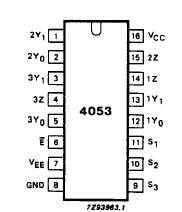
Pinout

  Connection Diagram


Specifications

SYMBOL PARAMETER MIN. MAX. UNIT CONDITIONS
VCC DC supply voltage -0.5 +11.0 V  
±IIK DC digital input diode current   20 mA for VI < -0.5 V or VI > VCC + 0.5 V
±ISK DC switch diode current   20 mA for VS < -0.5 V or VS > VCC + 0.5 V
±IS DC switch current   25 mA for -0.5 V < VS < VCC + 0.5 V
±IEE DC VEE current   20 mA  
±ICC; ±IGND DC VCC or GND current   50 mA  
Tstg storage temperature range -65 +150 °C  
Ptot power dissipation per package

plastic DIL
  750 mW for temperature range: -40 to + 125 °C
74HC/HCT
above + 70 °C: derate linearly with 12 mW/K
  plastic mini-pack (SO)   500 mW above + 70 °C: derate linearly with 8 mW/K
PS power dissipation per switch   100 mW  


Description

The 74HC/HCT4053 are high-speed Si-gate CMOS devices and are pin compatible with the "4053" of the "4000B" series. They are specified in compliance with JEDEC standard no. 7A.

The 74HC/HCT4053 are triple 2-channel analog multiplexers/demultiplexers with a common enable input (E). Each multiplexer/demultiplexer has two independent inputs/outputs (nY0 and nY1), a common input/output (nZ) and three digital select inputs (S1 to S3).

With E LOW, one of the two switches is selected (low impedance ON-state) by S1 to S3. With E HIGH, all switches are in the high impedance OFF-state, independent of S1 to S3. VCC and GND are the supply voltage pins for the digital control inputs (S1, to S3, and E). The VCC to GND ranges are 2.0 to 10.0 V for HC and 4.5 to 5.5 V for HCT. The analog inputs/outputs (nY0 and nY1, and nZ) can swing between VCC as a positive limit and VEE as a negative limit.VCC - VEE may not exceed 10.0 V. For operation of 74HC/HCT4053 as a digital multiplexer/demultiplexer, VEE is connected to GND (typically ground).


Customers Who Bought This Item Also Bought

Margin,quality,low-cost products with low minimum orders. Secure your online payments with SeekIC Buyer Protection.
Optical Inspection Equipment
Connectors, Interconnects
Tapes, Adhesives
803
Prototyping Products
DE1
Semiconductor Modules
View more