Isolation Voltage
:
Packaging
:
Maximum Operating Temperature
: + 125 C
Maximum Reverse Diode Voltage
: 5 V
Output Type
: Open Collector
Package / Case
: DIP-8
Maximum Forward Diode Voltage
: 1.7 V
Maximum Propagation Delay Time
: 100 us
Maximum Forward Diode Current
: 5 mA
Maximum Continuous Output Current
: 40 mA
Maximum Power Dissipation
: 200 mW
Minimum Operating Temperature
: - 55 C
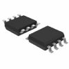
DescriptionThe HCPL-5731 is a high reliability Class H two channel hermetically sealed optocoupler in an 8-Pin DIP ceramic package with gold plated leads. Solder dipped leads and various lead forms are also available. See the datasheet for details.
The HCPL-5731 is capable of operation and storage over the full military temperature range and may also be purchased as either commercial grade, with full MIL-PRF-38534 Class Level K testing or from the the DSCC SMD 5962-89785. The HCPL-5731 is manufactured and tested on a MIL-PRF-38534 certified line and included in the DSCC Qualified Manufacturers List QML-38534 for Hybrid Microcircuits.
Each HCPL-5731 channel contains a GaAsP light emitting diode which is optically coupled to an integrated high gain photon detector. The high gain output stage features an open collector output providing both lower saturation voltage and higher signaling speed than possible with conventional photo-Darlington optocouplers. The shallow depth and small junctions offered by the HCPL-5731 IC process provides better radiation immunity than conventional photo transistor optocouplers.
The supply voltage can be operated as low as 2.0 V without adversely affecting the parametric performance. These HCPL-5731 devices have a 300% minimum CTR at an input current of only 0.5 mA making them ideal for use in low input current applications such as MOS, CMOS, low power logic interfaces or line receivers. Compatibility with high voltage CMOS logic systems is assured by specifying Icch and Ioh at 18 Volts.
Package styles for this die set in one, two or four channels are 8 and 16-Pin DIP through hole, 16-Pin surface mount DIP flat pack, and 20 pad leadless ceramic chip carrier. Most HCPL-5731 devices may be purchased with a variety of lead forms and plating options. See the datasheet for details.
Because the same electrical die (emitters and detectors) are used for each channel of each HCPL-5731 device listed in the datasheet, absolute maximum ratings, recommended operating conditions, electrical specifications, and performance characteristics shown in the datasheet figures are virtually identical for all parts. Occasional exceptions exist due to package variations and limitations and are as noted. Additionally, the same package assembly processes and materials are used in all devices. These similarities give justification for the use of data obtained from one part to represent other parts performance for reliability and certain limited radiation test results.

 HCPL-5731 Data Sheet


