Isolation Voltage
:
Maximum Continuous Output Current
:
Packaging
:
Maximum Operating Temperature
: + 125 C
Maximum Propagation Delay Time
: 500 ns
Maximum Forward Diode Voltage
: 1.8 V
Maximum Reverse Diode Voltage
: 5 V
Output Type
: Open Collector
Maximum Power Dissipation
: 295 mW
Package / Case
: DIP-8
Minimum Operating Temperature
: - 55 C
Maximum Forward Diode Current
: 18 mA
Features: • Performance Guaranteed over Full Military Temperature Range:-55 to +125
• Manufactured and Tested on a MILPRF-38534 Certified Line
• Hermetically Sealed Packages
• Dual Marked with Device Part Number and DSCC Drawing Number
• QML-38534
• HCPL-3120 Function Compatibility
• 2.0 A Minimum Peak Output Current
• 0.5V Maximum Low Level Output Voltage (VOL) Eliminates Need for Negative Gate Drive
• 10 kV/s Minimum Common Mode Rejection (CMR) at VCM = 1000V
• ICC = 5 mA Maximum Supply Current
• Under Voltage Lock-Out Protection (UVLO) with Hysteresis
• Wide Operating VCC Range: 15 to 30 Volts
• 500 ns Maximum Propagation Delay
• ± 0.35s Maximun Delay Between Devices
Application• Industrial and Military Environments
• High Reliability Systems
• Harsh Industrial Environments
• Transportation, Medical, and Life Critical Systems
• Uninterruptible Power Supplies (UPS)
• Isolated IGBT/MOSFET Gate Drive
• AC and Brushless DC Motor Drives
• Industrial Inverters
• Switch Mode Power Supplies (SMPS)Pinout Specifications
|
Parameter |
Symbol |
Min. |
Max. |
Units |
Note |
| Storage Temperature |
TS |
-65 |
+150 |
|
|
| Operating Temperature |
TA |
-55 |
+125 |
|
|
| Case Temperature |
TC |
|
+145 |
|
|
| Junction Temperature |
TJ |
|
+150 |
|
|
| Lead Solder Temperature |
|
|
260 for 10s |
|
|
| Average Input Current |
IFAVG |
|
25 |
mA |
1 |
Peak Transient Input Current
(<1 s pulse width, 300 pps) |
IFPK |
|
1.0 |
A |
|
| Reverse Input Voltage |
VR |
|
5 |
V |
|
| "High" Peak Output Current |
IOH(PEAK) |
|
2.5 |
A |
2 |
| "Low" Peak Output Current |
IOL(PEAK) |
|
2.5 |
A |
2 |
| Supply Voltage |
(VCC-VEE) |
0 |
35 |
V |
|
| Output Voltage |
VO(PEAK) |
0 |
VCC |
V |
|
| Emitter Power Dissipation |
PE |
|
45 |
mW |
1 |
| Output Power Dissipation |
PO |
|
250 |
mW |
3 |
| Total Power Dissipation |
PT |
|
295 |
mW |
4 |
Notes:
1. No derating required for typical case-to-ambient thermal resistance (CA=140/W). Refer to Figure 35.
2. Maximum pulse width = 10s, maximum duty cycle = 0.2%. This value is intended to allow for component tolerances for designs with IO peak minimum = 2.0A. See Applications section for additional details on limiting IOH peak.
3. Derate linearly above 102 free air temperature at a rate of 6mW/ for typical case-to-ambient thermal resistance (CA=140/W). Refer to Figure 36.
4. Derate linearly above 102 free air temperature at a rate of 6mW/ for typical case-to-ambient thermal resistance (CA=140/W). Refer to Figure 35 and 36.
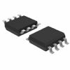
DescriptionThe HCPL-5121 is a high reliability Class H hermetically sealed optocoupler in an 8-Pin ceramic DIP package with gold plated leads. Solder dipped leads and various lead form options are also available. See the datasheet for details.
The HCPL-5121 is capable of operation and storage over the full military temperature range and may also be purchased in a commercial grade or from the DSCC Standard Microcircuit Drawing (SMD) 5962-04204. The HCPL-5121 is manufactured and tested on a MIL-PRF-38534 certified line and is included in the DSCC Qualified Manufacturers List QML-38534 for Hybrid Microcircuits.
The HCPL-5121 consists of a GaAsP LED optically coupled to an integrated circuit with a power output stage. The device is ideally suited for driving power IGBTs and MOSFETs used in motor control inverter applications. The high operating voltage range of the output stage provides the drive voltages required by gate controlled devices. The voltage and current supplied by this optocoupler makes it ideally suited for directly driving IGBTs with ratings up to 1200V/100A. For IGBTs with higher ratings, the HCPL-5121 can be used to drive a discrete power stage, which drives the IGBT gate.

 HCPL-5121 Data Sheet


